
Datasheet

Spartan-7 FPGAs Data Sheet: DC and AC Switching Characteristics
DS189 (v1.2) June 20, 2017 www.xilinx.com
Preliminary Product Specification 46
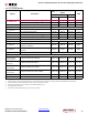
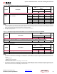
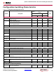
Conversion Rate
(4)
Conversion time:
continuous
t
CONV
Number of ADCCLK cycles. 26 – 32 Cycles
Conversion time: event t
CONV
Number of CLK cycles. – – 21 Cycles
DRP clock frequency DCLK DRP clock frequency. 8 – 250 MHz
ADC clock frequency ADCCLK Derived from DCLK. 1 – 26 MHz
DCLK duty cycle 40 – 60 %
XADC Reference
(5)
External reference V
REFP
Externally supplied reference voltage. 1.20 1.25 1.30 V
On-chip reference
Ground V
REFP
pin to AGND,
–40°C ≤ T
j
≤ 100°C
1.2375 1.25 1.2625 V
Ground VREFP pin to AGND,
–55°C ≤ T
j
< –40°C; 100°C < T
j
≤ 125°C
1.2251.251.275 V
Notes:
1. Offset and gain errors are removed by enabling the XADC automatic gain calibration feature. The values are specified for when this feature
is enabled.
2. Only specified for bitstream option XADCEnhancedLinearity = ON.
3. For a detailed description, see the ADC chapter in the 7 Series FPGAs and Zynq-7000 AP SoC XADC Dual 12-Bit 1 MSPS Analog-to-Digital
Converter User Guide (UG480) [Ref 8].
4. For a detailed description, see the Timing chapter in the 7 Series FPGAs and Zynq-7000 AP SoC XADC Dual 12-Bit 1 MSPS Analog-to-Digital
Converter User Guide (UG480) [Ref 8].
5. Any variation in the reference voltage from the nominal V
REFP
= 1.25V and V
REFN
= 0V will result in a deviation from the ideal transfer
function. This also impacts the accuracy of the internal sensor measurements (i.e., temperature and power supply). However, for external
ratiometric type applications allowing reference to vary by ±4% is permitted.
Table 50: XADC Specifications (Cont’d)
Parameter Symbol Comments/Conditions Min Typ Max Units