
Datasheet

Spartan-7 FPGAs Data Sheet: DC and AC Switching Characteristics
DS189 (v1.2) June 20, 2017 www.xilinx.com
Preliminary Product Specification 48
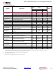
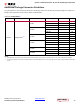
T
SMCSCCK
/
T
SMCCKCS
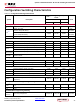
CSI_B setup/hold. 4.00/0.00 4.00/0.00 4.00/0.00 ns, Min
T
SMWCCK
/
T
SMCCKW
RDWR_B setup/hold. 10.00/0.00 10.00/0.00 10.00/0.00 ns, Min
T
SMCKCSO
CSO_B clock to out (330 Ω pull-up resistor
required).
7.00 7.00 7.00 ns, Max
T
SMCO
D[31:00] clock to out in readback. 8.00 8.00 8.00 ns, Max
F
RBCCK
Readback frequency. 100.00 100.00 100.00 MHz, Max
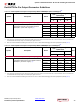
Boundary-Scan Port Timing Specifications
T
TAPTCK
/
T
TCKTAP
TMS and TDI setup/hold. 3.00/2.00 3.00/2.00 3.00/2.00 ns, Min
T
TCKTDO
TCK falling edge to TDO output. 7.00 7.00 7.00 ns, Max
F
TCK
TCK frequency. 66.00 66.00 66.00 MHz, Max
SPI Flash Master Mode Programming Switching
T
SPIDCC
/
T
SPICCD
D[03:00] setup/hold. 3.00/0.00 3.00/0.00 3.00/0.00 ns, Min
T
SPICCM
MOSI clock to out. 8.00 8.00 8.00 ns, Max
T
SPICCFC
FCS_B clock to out. 8.00 8.00 8.00 ns, Max
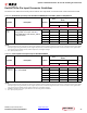
STARTUPE2 Ports
T
USRCCLKO
STARTUPE2 USRCCLKO input to CCLK output. 0.50/6.70 0.50/7.50 0.50/7.50 ns, Min/Max
F
CFGMCLK
STARTUPE2 CFGMCLK output frequency. 65.00 65.00 65.00 MHz, Typ
F
CFGMCLKTOL
STARTUPE2 CFGMCLK output frequency tolerance. ±50 ±50 ±50 %, Max
Device DNA Access Port
F
DNACK
DNA access port (DNA_PORT). 100.00 100.00 100.00 MHz, Max
Notes:
1. To support longer delays in configuration, use the design solutions described in the 7 Series FPGA Configuration User Guide (UG470) [Ref 9].
2. See the 7 Series FPGAs Overview (DS180) [Ref 1] for a list of devices that support bitstream encryption.
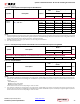
Table 51: Configuration Switching Characteristics (Cont’d)
Symbol Description
V
CCINT
Operating Voltage and Speed
Grade
Units
1.0V 0.95V
-2 -1 -1L