
Datasheet


7 Series FPGAs Data Sheet: Overview
DS180 (v2.5) August 1, 2017 www.xilinx.com
Product Specification 4
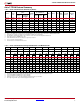
Kintex-7 FPGA Feature Summary
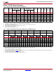
Table 6: Kintex-7 FPGA Feature Summary by Device
Device
Logic
Cells
Configurable Logic
Blocks (CLBs)
DSP
Slices
(2)
Block RAM Blocks
(3)
CMTs
(4)
PCIe
(5)
GTXs
XADC
Blocks
Total I/O
Banks
(6)
Max
User
I/O
(7)
Slices
(1)
Max
Distributed
RAM (Kb)
18 Kb 36 Kb Max (Kb)
XC7K70T 65,600 10,250 838 240 270 135 4,860 6 1 8 1 6 300
XC7K160T 162,240 25,350 2,188 600 650 325 11,700 8 1 8 1 8 400
XC7K325T 326,080 50,950 4,000 840 890 445 16,020 10 1 16 1 10 500
XC7K355T 356,160 55,650 5,088 1,440 1,430 715 25,740 6 1 24 1 6 300
XC7K410T 406,720 63,550 5,663 1,540 1,590 795 28,620 10 1 16 1 10 500
XC7K420T 416,960 65,150 5,938 1,680 1,670 835 30,060 8 1 32 1 8 400
XC7K480T 477,760 74,650 6,788 1,920 1,910 955 34,380 8 1 32 1 8 400
Notes:
1. Each 7 series FPGA slice contains four LUTs and eight flip-flops; only some slices can use their LUTs as distributed RAM or SRLs.
2. Each DSP slice contains a pre-adder, a 25 x 18 multiplier, an adder, and an accumulator.
3. Block RAMs are fundamentally 36 Kb in size; each block can also be used as two independent 18 Kb blocks.
4. Each CMT contains one MMCM and one PLL.
5. Kintex-7 FPGA Interface Blocks for PCI Express support up to x8 Gen 2.
6. Does not include configuration Bank 0.
7. This number does not include GTX transceivers.
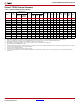
Table 7: Kintex-7 FPGA Device-Package Combinations and Maximum I/Os
Package
(1)
FBG484 FBG676
(2)
FFG676
(2)
FBG900
(3)
FFG900
(3)
FFG901 FFG1156
Size (mm) 23 x 23 27 x 27 27 x 27 31 x 31 31 x 31 31 x 31 35 x 35
Ball Pitch
(mm)
1.0 1.0 1.0 1.0 1.0 1.0 1.0
Device
GTX
(4)
I/O
GTX
(4)
I/O
GTX
I/O
GTX
(4)
I/O
GTX
I/O
GTX
I/O
GTX
I/O
HR
(5)
HP
(6)
HR
(5)
HP
(6)
HR
(5)
HP
(6)
HR
(5)
HP
(6)
HR
(5)
HP
(6)
HR
(5)
HP
(6)
HR
(5)
HP
(6)
XC7K70T 4 185 100 8 200 100
XC7K160T 4 185 100 8 250 150 8 250 150
XC7K325T 8 250 150 8 250 150 16 350 150 16 350 150
XC7K355T 24 300 0
XC7K410T 8 250 150 8 250 150 16 350 150 16 350 150
XC7K420T 28 380 0 32 400 0
XC7K480T
28 380 0 32 400 0
Notes:
1. All packages listed are Pb-free (FBG, FFG with exemption 15). Some packages are available in Pb option.
2. Devices in FBG676 and FFG676 are footprint compatible.
3. Devices in FBG900 and FFG900 are footprint compatible.
4. GTX transceivers in FB packages support the following maximum data rates: 10.3Gb/s in FBG484; 6.6Gb/s in FBG676 and FBG900. Refer to Kintex-7 FPGAs Data Sheet:
DC and AC Switching Characteristics (DS182
) for details.
5. HR = High-range I/O with support for I/O voltage from 1.2V to 3.3V.
6. HP = High-performance I/O with support for I/O voltage from 1.2V to 1.8V.