
Data Sheet


2/17/2018 Pcam 5C Reference Manual [Reference.Digilentinc]
https://reference.digilentinc.com/reference/add-ons/pcam-5c/reference-manual 7/11
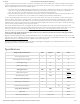
Voltage and Power Parameters Min Typical Max Units
Lens Chief Array Angle 24 Degrees
Shutter Type Rolling -
Sensitivity 600 mV/lux-sec
Pixel Size 1.4 x 1.4 μm
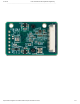
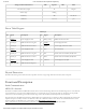
Header J1
Pin Signal Description Pin Signal Description
1 GND () Power Supply Ground 9 MIPI_CLK_P MIPI CSI-2 Clock Positive
2 LANE0_N MIPI CSI-2 Lane 0 Negative 10 GND () Power Supply Ground
3 LANE0_P MIPI CSI-2 Lane 0 Positive 11 PWUP Power supply and sensor enable
4 GND () Power Supply Ground 12 N/C Not Connected
5 LANE1_N MIPI CSI-2 Lane 1 Negative 13 SCL Serial Camera Control Bus (SCCB) Clock
6 LANE1_P MIPI CSI-2 Lane 1 Positive 14 SDA Serial Camera Control Bus (SCCB) Data
7 GND () Power Supply Ground 15 VCC3V3 Power Supply (3.3V) Input
8 MIPI_CLK_N MIPI CSI-2 Clock Negative
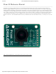
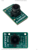
The PCB is 40 mm long and 25 mm wide. The 15-pin FFC connector is right angle and bottom mounted, with 1 mm pitch.
The Pcam 5C includes a dual-lane MIPI CSI-2 interface that is used to transmit image data from the OV5640 image sensor on the Pcam 5C
to the attached host. It consists of three differential pairs, two for data and one for a clock signal, which are all routed to the 15-pin FFC
connector. The clock and data signals are driven by the image sensor and should be treated as inputs by the attached host.
The physical layer of the MIPI CSI-2 interface is called D-PHY. It is supported by the I/O blocks on Xilinx Ultrascale devices natively, but
requires some passive circuitry external to the FPGA in order to be connected to Xilinx 7-series devices. For detailed information on the
circuitry required to use D-PHY with a 7-series device, see the XAPP894 Application Note
(https://www.xilinx.com/support/documentation/application_notes/xapp894-d-phy-solutions.pdf) available from Xilinx.
Pinout Table Diagram
Physical Dimensions
Functional Description
Serial Communication
MIPI CSI-2 Interface