
Data Sheet


2/17/2018 Pcam 5C Reference Manual [Reference.Digilentinc]
https://reference.digilentinc.com/reference/add-ons/pcam-5c/reference-manual 9/11
It is also possible to replace the included lens with a different M12 lens. Many suitable M12 lenses with a range of unique characteristics are
available for sale from third-party vendors. Care should be taken when choosing a third party lens to ensure it is appropriate to use with the
OV5640 image sensor and the Pcam 5C lens mount. Some longer lenses may make contact with the image sensor if over tightened, which
could cause damage.
Digilent recommends that the included lens never be fully removed unless a different lens is being swapped in. This will help prevent
damage to the image sensor, which is very delicate. If swapping in a different lens, the procedure should be done in a clean environment and
the time in which the image sensor is exposed should be minimized.
The PWUP signal on the 15-pin FFC connector is used by the host to turn the Pcam 5C on and off. It directly controls the power supplies
found on the Pcam 5C, disconnecting power to the OV5640 when it is not driven high. The PWUP signal must be driven high in order to
use the Pcam 5C.
The power-up sequence for the Pcam 5C includes a number of steps. These steps are implemented in the source code for the Pcam 5C
demo described in the Software Support section, however they are also provided here for reference purposes:
1. Execute a power-cycle by applying a low pulse of 100ms on CAM_PWUP, then driving it high.
2. Wait for 50ms.
3. Read sensor ID from registers 0x300A and 0x300B and check against 0x56 and 0x40, respectively.
4. Choose system input clock from pad by writing 0x11 to register address 0x3103.
5. Execute software reset by writing 0x82 to register address 0x3008.
6. Wait for 10ms.
7. De-assert reset and enable power down until configuration is done by writing 0x42 to register address 0x3008.
8. Choose system input clock from PLL by writing 0x03 to register address 0x3103.
9. Set PLL registers for desired MIPI data rate and sensor timing (frame rate).
10. Set imaging configuration registers.
11. Enable MIPI interface by writing either 0x45 for two-lane mode or 0x25 for one-lane mode to register address 0x300E.
12. Let MIPI clock free-run, and force LP11 when no packet transmission by writing 0x14 to register address 0x4800.
13. Set output format to RAW10 by writing 0x00 to register address 0x4300 and 0x03 to register address 0x501F.
14. Wake up sensor by writing 0x02 to register address 0x3800.
The procedure above can be repeated at any time during execution to perform a reset on the sensor.
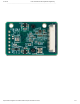
The unloaded header labeled J3 on the Pcam 5C can be used to access some additional signals of the OV5640. This is so that those with
access to the OV5640 datasheet can use some of the additional functionality they provide. These signals will not be useful to those without
access to the OV5640 datasheet, as they are otherwise undocumented. Most will not need to have any use for the functionality provided on
these signals, and their use is not required for normal function of the Pcam 5C.
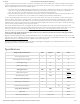
The signals are briefly described in the table below.
Header J3
Pin Signal Description Pin Signal Description
1 GPIO0 Camera GPIO () 0 5 GND () Power Supply Ground
2 GPIO1 Camera GPIO () 1 6 VCMSINK Auto-focus voice coil motor sink
3 FREX Frame exposure mode shutter signal 7 VCMGND Auto-focus voice coil motor ground
4 STROBE Flash LED () strobe signal
Power-up and Reset
Auxiliary Signals
Liquid Lens Support