
User manual


22.8.2018 Cora Z7 Reference Manual [Reference.Digilentinc]
https://reference.digilentinc.com/reference/programmable-logic/cora-z7/reference-manual 18/20
The pins labeled A0-A11 and V_P/V_N are used as analog inputs to the XADC module of the FPGA. The FPGA expects that the
inputs range from 0-1 V. On the pins labeled A0-A5, the Cora Z7 uses an external circuit to scale down the input voltage from 3.3V.
This circuit is shown in Figure 13.2.1. This circuit allows the XADC module to accurately measure any voltage between 0V and 3.3V
(relative to the Cora Z7's GND ()) that is applied to any of these pins. The pins labeled A0-A5 can also be used as digital inputs or
outputs, as they are also connected directly to the FPGA before the resistor divider circuit (also shown in Figure 13.2.1).
(https://reference.digilentinc.com/_media/reference/programmable-logic/cora-z7/cora-analog-single-ended.png) Figure 13.2.1. Single-Ended Analog
Inputs
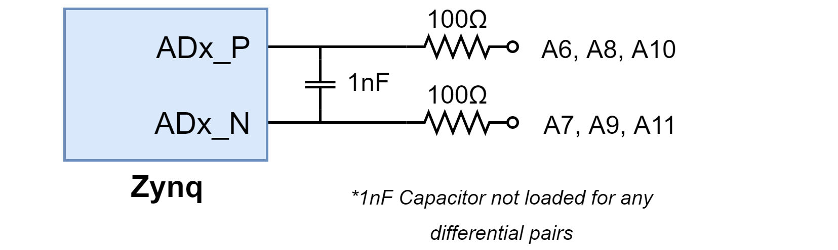
The pins labeled A6-A11 are connected directly to 3 pairs of analog capable pins on the FPGA via an anti-aliasing filter. This circuit is
shown in Figure 13.2.2. These pairs of pins can be used as differential analog inputs with a voltage difference between 0-1V. The even-
numbered pins are connected to the positive pins of the trio and the odd numbers are connected to the negative pins (so A6 and A7
form an analog input pair with A6 being positive and A7 being negative). Note that though the pads for the capacitor are present, they
are not loaded for these pins. Since the analog capable pins of the FPGA can also be used like normal digital FPGA pins, it is also
possible to use these pins for Digital I/O.
(https://reference.digilentinc.com/_media/reference/programmable-logic/cora-z7/cora-analog-differential.png) Figure 13.2.2. Differential Analog
Inputs
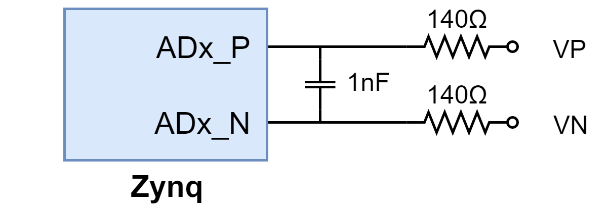
The pins labeled V_P and V_N are connected to the VP_0 and VN_0 dedicated analog inputs of the FPGA. This pair of pins can also be
used as a differential analog input with voltage between 0-1V, but they cannot be used as Digital I/O. The capacitor in the circuit shown
in Figure 13.2.3 for this pair of pins is loaded on the Cora Z7.
(https://reference.digilentinc.com/_media/reference/programmable-logic/cora-z7/cora-analog-dedicated.png) Figure 13.2.3. Dedicated Analog Input
Pair
The XADC core within the Zynq is a dual channel 12-bit analog-to-digital converter capable of operating at 1 MSPS. Either channel can
be driven by any of the analog inputs connected to the shield pins. The XADC core is controlled and accessed from a user design via
either the Dynamic Reconfiguration Port (DRP) or an AXI interface connected to the Zynq PS. These interfaces also provide access to
voltage monitors that are present on each of the FPGA’s power rails, and a temperature sensor that is internal to the FPGA. For more
information on using the XADC core, refer to the Xilinx document titled “7 Series FPGAs and Zynq-7000 All Programmable SoC
XADC Dual 12-Bit 1 MSPS Analog-to-Digital Converter”. A demo that uses the XADC core is available through the Cora Z7 Resource
Center (https://reference.digilentinc.com/reference/programmable-logic/cora-z7/start).