Zmod ADC Reference Manual The Digilent Zmod ADC () is an open-source hardware SYZYGY™ 1)compatible pod containing a dual-channel ADC () and the associated front end. The Zmod ADC () is intended to be used with any SYZYGY™ compatible carrier board having the required capabilities.
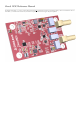
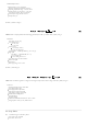
Figure 1. Zmod ADC top and bottom views. [] The analog inputs can be connected to a circuit using SMA cables. Driven by the SYZYGY™ carrier, the Zmod ADC () can acquire two simultaneous signals (1MΩ, ±25V, single-ended, 14-bit, 100MS/s, 70MHz+ bandwidth).
The Zmod ADC () was designed to be a piece in a modular, HW and SW open-source ecosystem. Combined with a SYZYGY™ carrier, other SYZYGY™ compatible pods, Zmod ADC () can be used for a variety of applications: data acquisition systems, closed loop controllers, scopes, etc. Features Channels: 2 Channel type: single ended Resolution: 14-bit Input range: ±1V (Low Range) or ±25V (High Range) Absolute Resolution: 0.13mV (Low Range) or 3.21mV (High Range) Accuracy: ±0.
The high gain is: VSC−H G VSCOP E−SM A = R4 + R6 = 0.96 R2 + R4 + R6 (4) The Low Range (at high gain): −1V ≤ VSCOP E−SM A ≤ 1V (5) The two dividers are designed to have the same equivalent impedance (both active and reactive): Rech = R1 + R3 + R5 = R2 + R4 + R6 = 1M ohm (6) Experiments shown that there are significant parasitic capacities of the layout and buffer input stage: CPH (high gain divider), parallel to C6, and CPL (low gain divider), parallel to C7.
Figure 4. Relay Drivers. [] IC14 and IC15 in Fig. 5 are 74LVC07ABQ open-drain gates used as level translators from VADJ = 1.8V to VCC5V0 = 5V. 5 V tolerant inputs and outputs (open-drain) for interfacing with 5 V logic Wide supply voltage range from 1.2 V to 5.5 V CMOS low power consumption Direct interface with TTL levels Inputs accept voltages up to 5 V Complies with JEDEC standard: JESD8-7A (1.65 V to 1.95 V) JESD8-5A (2.3 V to 2.7 V) JESD8-C/JESD36 (2.7 V to 3.
ADR3412ARJZ features: Initial accuracy: ±0.1% (maximum) Maximum temperature coefficient: 8 ppm/°C Operating temperature range: −40°C to +125°C Output current: +10 mA source/−3 mA sink Low quiescent current: 100 μA (maximum) Low dropout voltage: 250 mV at 2 mA Output noise (0.1 The ADC () reference voltage is: VREF ADC = VREF 1V 2SC ∗ R73 = 1V (23) R71 + R73 An ADA4841-2 OpAmp buffers the VCM voltage generated by the ADC () to feed the ADC () buffer, in Fig. 8. ADA4841-2 Low power: 1.
Low Distortion (HD2/HD3): –80dBc/–69dBc at 50MHz, 2VP-P –104dBc/–90dBc at 20MHz, 2VP-P Rail-to-Rail Differential Input 2.7V to 3.5V Supply Voltage Range Fully Differential Input and Output Adjustable Output Common Mode Voltage 800MHz –3dB Bandwidth with AV = 1 Gain-Bandwidth Product: 3GHz Low Power Shutdown Available in 8-Lead MSOP and Tiny 16-Lead 3mm × 3mm × 0.
VOU T max sat < 2.5V (36) Resulting a stress value at the ADC () input: VADC max sat = VOU T max sat ∗ Gdiv = 1.865V (37) which is less than the allowed voltage at the ADC () input = 2.1V. 2.5. Scope ADC The Zmod ADC () uses a dual channel, high speed, low power, 14-bit, 105MS/s ADC () (Analog part number AD9648, as shown in Fig. 11. The important features of AD9648: SNR = 74.
N ⋅ Range ⋅ (1 + CG) Vin = 2 + CA 13 (45) were: N = the 14 bit, 2's complement integer number returned by the ADC () Vin= the corrected value of the input voltage CA = calibration Additive constant (for the appropriate channel and gain; see Table 3) CG = calibration Gain constant (for the appropriate channel and gain; see Table 3) Range= the ideal Range of the Scope input stage (approximation of the values in equation 40): 1.086 (for low range: ±1V) or 26.25 (for high range: ±25V) 2.
Contents Type Size(Bytes) Value Address DNA full data length uint16 2 91 0x8000 DNA header length uint16 2 40 0x8002 SYZYGY DNA major version uint8 1 1 0x8004 SYZYGY DNA minor version uint8 1 0 0x8005 Required SYZYGY DNA major version uint8 1 1 0x8006 Required SYZYGY DNA minor version uint8 1 0 0x8007 Maximum operating 5V load (mA) uint16 2 400 0x8008 Maximum operating 3.
0.1% resistors and 1% capacitors in all the critical analog signal paths Capacitive trimmers for balancing the Scope Input Divider and Gain Selection No other mechanical trimmers (as these are big, expensive, unreliable and affected by vibrations, aging, and temperature drifts) Software calibration, at manufacturing User software calibration, as an option A software calibration is performed on each device as a part of the manufacturing test. Reference signals are connected to the Scope inputs.
The internal analog rails sequence is: AVCC1V8 - ADC () analog rail AVCC3V0 - ADC () driver AVCC-2V5, AVCC4V5 - Scope buffer, reference voltage 4.1. AVCC1V8 The analog supply AVCC1V8 is built from VCC5V0 using IC21, an ADP2138Fixed Output Voltage, 800mA, 3MHz, Step-Down DC-to-DC converter. To insure low output voltage ripple a second LC filter (FB9 in Fig. 9) is added and forced PWM mode is selected. Input voltage: 2.3 V to 5.
Adjustable-output voltage range 0.8 V to 5.0 V (ADP123) Excellent PSRR performance: 60 dB at 100 kHz () Excellent load/line transient response Optimized for small 1.0 μF ceramic capacitors Current limit and thermal overload protection Logic controlled enable Compact packages: 5-lead TSOT and 6-lead 2 mm × 2 mm LFCSP 4.4. AVCC-2V5 The AVCC-2V5 analog power supply is implemented with the ADP2301 Step-Down regulator in an inverting Buck-Boost configuration.
Parameter Value VIO supply voltage 1.8V Maximum VIO supply current 270mA Total number of I/O 28 Number of differential I/O pairs 0 Width Single Written by Mircea Dabacan, PhD, Technical University of Cluj-Napoca Romania 1) The “SYZYGY™ ” mark is owned by Opal Kelly.


