
User Manual
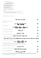


The internal analog rails sequence is:
AVCC1V8 -
ADC () analog rail
AVCC3V0 -
ADC () driver
AVCC-2V5, AVCC4V5 - Scope buffer, reference voltage
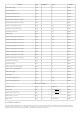
Input voltage: 2.3 V to 5.5 V
Peak efficiency: 95%
3
MHz () fixed frequency operation
Typical quiescent current: 24 μA
Very small solution size
6-lead, 1 mm × 1.5 mm WLCSP package
Fast load and line transient response
100% duty cycle low dropout mode
Internal synchronous rectifier, compensation, and soft start
Current overload and thermal shutdown protections
Ultra-low shutdown current: 0.2 μA (typical)
Forced PWM and automatic PWM/PSM modes
Input voltage supply range: 2.3 V to 5.5 V
300 mA maximum output current
Fixed and adjustable output voltage versions
Very low dropout voltage: 85 mV at 300 mA load
Low quiescent current: 45 µA at no load
Low shutdown current: <1 µA
Initial accuracy: ±1% accuracy
Up to 31 fixed-output voltage options available from
1.75 V to 3.3 V
Adjustable-output voltage range
0.8 V to 5.0 V (ADP123)
Excellent PSRR performance: 60 dB at 100 kHz ()
Excellent load/line transient response
Optimized for small 1.0 μF ceramic capacitors
Current limit and thermal overload protection
Logic controlled enable
Compact packages: 5-lead TSOT and 6-lead 2 mm × 2 mm LFCSP
Input voltage supply range: 2.3 V to 5.5 V
300 mA maximum output current
Fixed and adjustable output voltage versions
Very low dropout voltage: 85 mV at 300 mA load
Low quiescent current: 45 µA at no load
Low shutdown current: <1 µA
Initial accuracy: ±1% accuracy
Up to 31 fixed-output voltage options available from
1.75 V to 3.3 V
4.1. AVCC1V8
The analog supply AVCC1V8 is built from VCC5V0 using IC21, an
ADP2138Fixed Output Voltage, 800mA, 3MHz, Step-Down DC-to-DC converter.
To insure low output voltage ripple a second LC filter (FB9 in Fig. 9) is added and forced PWM mode is selected.
4.2. AVCC3V0
The analog supply AVCC3V0 is built from VCC3V3 using IC22, an
ADP1225.5 V Input, 300 mA, Low Quiescent Current, CMOS Linear Regulator,
Fixed Output Voltage. To reduce noise and reduce the crosstalk between supplied circuits, the rail uses individual LC filters: FB3 in Fig. 10, FB6
(Channel 2 ADC () Driver - not shown), FB7 in Fig. 7.
4.3. AVCC4V5
The analog supply AVCC4V5 is built from VCC5V0 using IC19, an
ADP123 5.5 V Input, 300 mA, Low Quiescent Current, CMOS Linear Regulator,
Adjustable Output Voltage. To reduce noise and reduce the crosstalk between supplied circuits, the rail uses individual LC filters: FB2 in Fig. 6, FB5
(Channel 2 ADC () Buffer - not shown), FB8 in Fig. 9.