
User Manual


Adjustable-output voltage range
0.8 V to 5.0 V (ADP123)
Excellent PSRR performance: 60 dB at 100
kHz ()
Excellent load/line transient response
Optimized for small 1.0 μF ceramic capacitors
Current limit and thermal overload protection
Logic controlled enable
Compact packages: 5-lead TSOT and 6-lead 2 mm × 2 mm LFCSP
1.2 A maximum load current
±2% output accuracy over temperature range
1.4
MHz () switching frequency
High efficiency up to 91%
Current-mode control architecture
Output voltage from 0.8 V to 0.85 × VIN
Automatic PFM/PWM mode switching
Integrated high-side MOSFET and bootstrap diode,
Internal compensation and soft start
Undervoltage lockout (UVLO), Overcurrent protection (OCP) and thermal shutdown (TSD)
Available in ultrasmall, 6-lead TSOT package
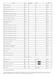
Power rails
VCC5V0
VCC3V3
VADJ - needs to be set by the carier board to 1.8V
GND ()
Shield
SYZYGY™ I2C bus:
MCU_SCLUSCK
MCU_SDA_
MOSI ()
ADC () differential input clock
CLKIN_ADC ()_P
CLKIN_
ADC ()_N
ADC () single ended output clock:
CLKOUT_ADC () (coupled with
GND
() in the differential P2C pair)
R_GA for geographical address identification
SYNC_
ADC () for ADC () internal clock divider synchronization
ADC () data bus: DOUT_ADC ()_0…13
ADC () SPI bus:
CS ()_SC1n
SCLK ()_SC
SDIO_SC
relay control
SCx_yy_z
P
arameter Value
Maximum 5V supply current 400mA
Maximum 3.3V supply current 100mA
4.4. AVCC-2V5
The AVCC-2V5 analog power supply is implemented with the
ADP2301 Step-Down regulator in an inverting Buck-Boost configuration. See application
Note
AN-1083: Designing an Inverting Buck Boost Using the ADP2300 and ADP2301 . To reduce noise and reduce the crosstalk between supplied
circuits, the rail uses individual LC filters: FB1 in Fig. 6, FB4 (Channel 2 ADC () Buffer - not shown). The ADP2301 features:
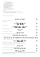
5. The SYZYGY™ Connector
The SYZYGY™ connector in
provides the interface with the carrier board. The used signals are:
6.
The SYZYGY™ compatibility table
Table 6. The SYZYGY™ compatibility table []