
User Manual
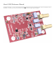
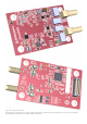


The Zmod
ADC () was designed to be a piece in a modular, HW and SW open-source ecosystem. Combined with a SYZYGY™ carrier, other SYZYGY™
compatible pods, Zmod
ADC () can be used for a variety of applications: data acquisition systems, closed loop controllers, scopes, etc.
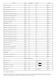
Channels: 2
Channel type: single ended
Resolution: 14-bit
Input range: ±1V (Low Range) or ±25V (High Range)
Absolute Resolution: 0.13mV (Low Range) or 3.21mV (High Range)
Accuracy: ±0.2% of Range
Sample rate (real time): 100MS/s
Input impedance: 1MΩ||18pF
Analog bandwidth: 70
MHz ()+ @ 3dB, 30 MHz () @ 0.5dB, 20 MHz () @ 0.1dB
Input protected to: ±50V
Input Divider and Gain Selection: high bandwidth input adapter/divider. High or low-gain can be selected by the FPGA
Buffer: high impedance buffer
Driver: pro
vides appropriate signal levels and protection to the
ADC ().
Scope Reference: generates and buffers reference v
oltages for the scope stages
ADC (): the analog-to-digital converter for both scope channels.
The Power Supplies and Control block g
enerates all internal supply voltages.
The MCU works as a I2C memory for two different purposes:
The DNA includes the standard
SYZYGY™ (https://syzygyfpga.io) pod identification information.
The Calibration Memory stores all calibration parameters. Except for the “Probe Calibration” trimmers in the scope Input divider, the
Zmod
ADC () includes no analog calibration circuitry. Instead, a calibration operation is performed at manufacturing (or by the user), and
parameters are stored in memory. The application software uses these parameters to correct the acquired data and the generated signals
In the sections that follow, schematics are not shown separately for identical blocks. For example, the Scope Input Divider and Gain Selection schematic is
only shown for channel 1 since the schematic for channel 2 is identical. Indexes are omitted where not relevant. As examples, in equation below,
does not contain the channel index (because the equation applies to both channels 1 and 2).
Fig. 3 shows the scope input divider and gain selection stage.
C and C are capacitive trimmers, 3…10pF, -0/+50% tolerance. The worse case range is 4.5…10pF. All other capacitors are 1% tolerance, all the resistors
are 0.1%.
The IC1 relay switches between two symmetrical R-C dividers. Each of them provide:
Scope input impedance = 1MOhm || 18pF
Two different attenuations for high-gain/low-gain (25:1)
Controlled capacitance, much higher than the parasitical capacitance of subsequent stages
Constant attenuation over a large frequency range (trimmer adjusted)
The maximum voltage rating for scope inputs is limited to:
The DC low gain is:
The High Range (at low gain):
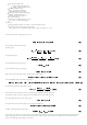
Features
1. Architectural Overview and Block Diagram
This document describes the Zmod ADC ()'s circuits, with the intent of providing a better understanding of its electrical functions, operations, and a more
detailed description of the hardware’s features and limitations. It is not intended to provide enough information to enable complete duplication of the Zmod
ADC (), but can help users to design custom configurations for programmable parts in the design.
Zmod ADC ()'s block diagram is presented in Fig. 2 below. The core of the Analog Zmod ADC () is the dual channel, high speed, low power, 14-bit,
105MS/s ADC (),
AD9648. The carrier board is responsible to configure the internal registers of the ADC () circuit, provide the acquisition clock and
receive the data.
The Analog Input block is also called the Scope, because of similar structure and behavior to such a front end. The signals in this circuitry use a “SC”
indexes to indicate they are related to the scope block. Signals and equations also use certain naming conventions. Analog voltages are prefixed with a “V”
(for voltage), and suffixes and indexes are used in various ways: to specify the location in the signal path (IN, MUX, BUF, ADC (), etc.); to indicate the
related instrument (SC, etc.); to indicate the channel (1 or 2); and to indicate the type of signal (P, N, or diff). Referring to the block diagram in Fig. 2 below:
1
V
SCOPE
−
SMA
2. Scope
2.1. Scope Input Divider and Gain Selection
5 6
−50
V
<
V
SCOPE
−
SMA
< 50
V
(1)
= = 0.04 (2)
V
SC
−
LG
V
SCOPE
−
SMA
R
5
R
1
+
R
3
+
R
5
−25
V
≤
V
SCOPE
−
SMA
≤
25
V
(3)