
User Manual


The high gain is:
The Low Range (at high gain):
The two dividers are designed to have the same equivalent impedance (both active and reactive):
Experiments shown that there are significant parasitic capacities of the layout and buffer input stage: C (high gain divider), parallel to C , and C (low
gain divider), parallel to C . The trimmers should compensate for these parasitic capacities and adjust for perfect matching:
With the chosen values, the correct adjustment results in about mid-position of trimmers C and C :
which solves the parasitic capacities as:
The Low Gain and High Gain dividers have very close equivalent capacitance, within the tolerances and model approximations:
Experiments show that the equivalent capacitances are even closer than the values above, about 18pF. The computing error mainly derives from trimmer
position approximation.
The IC2 relay shorts the C1 capacitor when DC coupling is desired. Otherwise, C1 forms a High Pass filter with the selected divider, for AC coupling, with
the corner frequency:
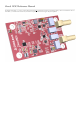
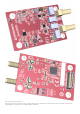
IC1 and IC2 in Fig. 3, are HFD4/4.5L latching relays possible replacement: IM42GR
The schematic
shows the “reset” position. A relay is “set” when a positive voltage is applied at the coil terminals and it is “reset” when a negative voltage is
applied (see the polarity on the schematic symbol). The relay keeps state when no current flows trough the coil (the terminals are driven at the same voltage
or at least one of the terminals is “open”). The nominal coil voltage is 4.5V.
The IC16, IC17 and IC18 in Fig. 4 are A3910EEETR-T drivers for the relays.
They feature:
Low RDS(on) outputs
Standby mode with zero current drain
Small 2 × 2 DFN package
Crossover Current protection
Thermal Shutdown protection
Normally, all of them have both HIN and LIN inputs “low” or both “High” driving the “OUT” pins “High Z”. To “set” a relay, OUT2 of IC16 is set
“Low” (HIN=“Low”, LIN=“High”) and the corresponding OUT pin of IC17 or IC18 is set “High” (HIN=“High”, LIN=“Low”). All other OUT pins are
set “High Z”. To “reset” a relay, OUT2 of IC16 is set “High” (HIN=“High”, LIN=“Low”) and the corresponding OUT pin of IC17 or IC18 is set “Low”
(HIN=“Low”, LIN=“High”). All other OUT pins are set “High Z”.
= = 0.96 (4)
V
SC
−
HG
V
SCOPE
−
SMA
R
4
+
R
6
R
2
+
R
4
+
R
6
−1
V
≤
V
SCOPE
−
SMA
≤ 1
V
(5)
R
ech
=
R
1
+
R
3
+
R
5
=
R
2
+
R
4
+
R
6
= 1
Mohm
(6)
PH 6 PL
7
C
3
∗
R
2
= (
C
PH
+
C
6
) ∗ (
R
4
+
R
6
) (7)
(
C
PH
+
C
6
) = = 18
pF
(8)
C
3
∗
R
2
R
4
+
R
6
(
C
4
+
C
5
) ∗ (
R
1
+
R
3
) = (
C
PL
+
C
7
) ∗
R
5
(9)
(
C
PL
+
C
7
) = (
C
4
+
C
5
) ∗ (10)
(
R
1
+
R
3
)
R
5
5 6
C
5
=
C
6
= 7
pF
(11)
C
PH
= 11
pF
(12)
C
PL
= 8.8
pF
(13)
C
HGech
= =
C
ech
= 17.28
pF
(14)
C
3
∗
R
2
R
2
+
R
4
+
R
6
C
LGech
= = 16.03
p
(15)
(
C
7
+
C
PL
) ∗
R
5
R
1
+
R
3
+
R
5
C
ech
= 18
p
(16)
f
c
= ≈ = 10.6
Hz
(17)
1
2 ∗
π
∗
R
ech
∗ (
C
ech
+
C
1
)
1
2 ∗
π
∗
R
ech
∗
C
1