
User Manual


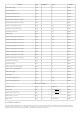

5 V tolerant inputs and outputs (open-drain) for interfacing with 5 V logic
Wide supply voltage range from 1.2 V to 5.5 V
CMOS low power consumption
Direct interface with TTL levels
Inputs accept voltages up to 5 V
Complies with JEDEC standard:
JESD8-7A (1.65 V to 1.95 V)
JESD8-5A (2.3 V to 2.7 V)
JESD8-C/JESD36 (2.7 V to 3.6 V)
ESD protection:
HBM JESD22-A114F exceeds 2000 V
MM JESD22-A115-B exceeds 200 V
CDM JESD22-C101E exceeds 1000 V
Specified from -40 °C to +85 °C and -40 °C to +125 °C
A non-inverting ADA4817 stage provides very high impedance as load for the input divider.
High speed
−3 dB bandwidth (G = 1, RL = 100 Ω): 1050 MHz ()
Slew rate: 870 V/µs
0.1% settling time: 9 ns
Input bias current: 2 pAtypical
Input capacitance
Common-mode capacitance: 1.3 pF typical
Differential mode capacitance: 0.1 pF typical
Low input noise
Voltage noise: 4 nV/√Hz at 100 kHz ()
Current noise: 2.5 fA/√Hz at 100 kHz ()
Low distortion: −90 dBc at 10 MHz () (G = 1, RL = 1 kΩ)
Linear output current: 40 mA
Supply quiescent current per amplifier: 19 mAtypical
Powered down supply quiescent current per amplifier: 1.5 mAtypical
The maximum output voltage swing is:
The gain is:
The actual input and output range (for nominal usage) is:
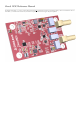
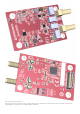
Figure 4. Relay Drivers. []
IC14 and IC15 in Fig. 5 are
74LVC07ABQ open-drain gates used as level translators from VADJ = 1.8V to VCC5V0 = 5V.
2.2. Scope Buffer
The
ADA4817 is supplied +4.5V/-2.5V.
The maximum input voltage swing is:
−2.5
V
<
V
SC
−
HLG
< 1.7
V
(18)
−1.3
V
<
V
BUFF
< 3.1
V
(19)
= 1 (20)
V
BUFF
V
SC
−
HLG
−1
V
<
V
SC
−
HLG
=
V
BUFF
< 1
V
(21)
The
ADA4817 data sheet does not include any explicit or implicit mention of input protection diodes, nor about the maximum current supported by
such diodes, so external D1 was added in the schematic for safety. However, the leakage current of D1 adds significant error and experiments proved that
the input protection diodes do exist within the
ADA4817, so D1 is a “No Load”.
The Zmod ADC () is specified to resist to accidental input voltages up to +/-50V. In these cases, the buffer input voltage is limited by the protection diodes
at 0.6V above the AVCC4V5 or below AVCC-2V5. The protection current is limited by R2 (at High Gain) or R1+R3 (at Low Gain) (see the input divider
= = −1.18
mA
(22)
SCOPE
−
SMA
−
V
AV CC
−2
V
5
−50
V
+ 2.5
V
40.2
kohm
2.3. Scope Reference
In Fig. 7, a low noise reference,
ADR3412ARJZ and an
ADA4841-2 OpAmp are used to generate 1V reference voltage for the ADC ().