
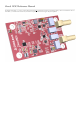
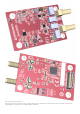
User Manual


Low Distortion (HD2/HD3):
–80dBc/–69dBc at 50MHz, 2VP-P
–104dBc/–90dBc at 20MHz, 2VP-P
Rail-to-Rail Differential Input
2.7V to 3.5V Supply Voltage Range
Fully Differential Input and Output
Adjustable Output Common Mode Voltage
800MHz –3dB Bandwidth with AV = 1
Gain-Bandwidth Product: 3GHz
Low Power Shutdown
Available in 8-Lead MSOP and Tiny 16-Lead
3mm × 3mm × 0.75mm QFN Packages
It is used for:
Driving the differential inputs of the
ADC () (with low impedance outputs)
Providing the common mode voltage for the
ADC ()
ADC () protection: IC2 is supplied 3V, while the ADC () inputs only support -0.1…2.1V.
The input common mode voltage range is rail-to-rail:
The actual input common mode voltage is:
The driver gain is:
The output divider gain:
The nominal Driver input voltage range is:
The nominal Driver output voltage range is:
With a unity common mode gain, the driver output common mode voltage is:
The nominal Buffer output single ended voltage range is:
The maximum nominal driver single ended current is:
which is below the data sheet limit of 5mA, for covering the driver single ended voltage range above.
For passing at the
ADC () input, the voltages above are multiplied by the resistive divider gain of G .
The nominal differential
ADC () input voltage range is:
The output divider common mode voltage is close to the recommended 0.9V:
The
ADC () input single ended voltage range is:
For the
ADC () input protection, the maximum driver single ended voltage should be considered. The driver amplifier datasheet only specifies the linear
output voltage range. There is no information about the worst case saturated output voltages. Based on the data sheet and measurements, the driver
maximum saturated single ended voltage was estimated to:
0
V
≤
V
+
LTC
6406
=
V
−
LTC
6406
≤ 3
V
(25)
G
drv
= = = = 1.27 (26)
V
OUTdiff
V
BUFF
R
11
R
12
R
19
R
14
G
div
= = = = 0.746 (27)
V
ADCdiff
V
OUTdiff
R
16
R
13
+
R
16
R
17
R
15
+
R
17
−1
V
<
V
BUFF
< 1
V
(28)
−1.27
V
<
V
OUT diff
< 1.27
V
(29)
V
CMOUT
= (
V
OUT
+
+
V
OUT
−
)/2 =
V
CMSC
= 1.2
V
(30)
V
CMOUT
−
V
OUT diff
/2 = 1.2
V
− 1.27/2 = 0.565
V
<
V
OUT
+
,
V
OUT
−
<
V
CMOUT
+
V
OUT diff
/2 = 1.2
V
+ 1.27/2 = 1.835
V
(31)
I
OUT max
= = = 4.65
mA
(32)
V
OUT max
R
13
+
R
16
1.835
V
394
ohm
div
−1
V
<
V
ADC diff
< 1
V
(33)
V
CMADC
= (
V
ADCP
+
V
ADCN
)/2 = 0.895
V
(34)
0.395
V
<
V
ADCP
,
V
ADCN
< 1.395
V
(35)