
User Manual


Resulting a stress value at the
ADC () input:
which is less than the allowed voltage at the
ADC () input = 2.1V.
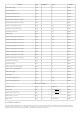
SNR = 74.5dBFS @70
MHz ()
SFDR =91dBc @70 MHz ()
Low power: 78mW/channel ADC () core@ 125MS/s
Differential analog input with 650 MHz () bandwidth
IF sampling frequencies to 200 MHz ()
On-chip voltage reference and sample-and-hold circuit
2 V p-p differential analog input
DNL = ±0.35 LSB
Serial port control options
Offset binary, gray code, or two's complement data format
Optional clock duty cycle stabilizer
Integer 1-to-8 input clock divider
Data output multiplex option
Built-in selectable digital test pattern generation
Energy-saving power-down modes
Data clock out with programmable clock and data alignment
The differential inputs are driven via a low-pass filter comprised of C114 together with R13, R15, R16, R17 in the buffer stage. The differential clock is AC-
coupled and the line is impedance matched. The clock is internally divided by 4 to operate the
ADC () at a constant 100 MHz () sampling rate. The ADC ()
generates the common mode reference voltage (VCM_SC) to be used in the buffer stage.
The digital stage of the
ADC () and the corresponding FPGA bank are supplied at 1.8V by the SYZYGY™ voltage V .
The multiplexed mode is used, to combine the two channels on a single data bus and minimize the number of used FPGA pins. CLKOUT_SC is provided
to the FPGA for synchronizing data.
Combining Gain equations , , , , and from previous chapters, the total scope gains are:
Considering the
ADC () input voltage range shown in :
To cover component value tolerances and to allow software calibration, only the ranges below are specified.
With the 14-bit
ADC (), the absolute resolution of the scope is:
For V voltage value at the input of the Scope channel, the ZmodADC sends a signed 14 bit integer, N. This value is used to compute V :
V
OUT max sat
< 2.5
V
(36)
V
ADC max sat
=
V
OUT max sat
∗
G
div
= 1.865
V
(37)
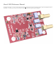
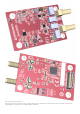
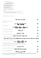
2.5. Scope ADC
The Zmod ADC () uses a dual channel, high speed, low power, 14-bit, 105MS/s ADC () (Analog part number
AD9648, as shown in Fig. 11.
The important features of AD9648:
adj
2.6. Scope Signal Scaling
2 4 20 26 27
Low gain
= = 0.038 (38)
V
ADC diff
V
SCOPE
−
SMA
High gain
= = 0.91 (39)
V
ADC diff
V
SCOPE
−
SMA
33
at low gain
: −26.3
V
<
V
SCOPE
−
SMA
< 26.3
V
at high gain
: −1.1
V
<
V
SCOPE
−
SMA
< 1.1
V
(40)
at low gain
: −25
V
<
V
SCOPE
−
SMA
< 25
V
(41)
at high gain
: −1
V
<
V
SCOPE
−
SMA
< 1
V
(42)
at low gain
: = 3.21
mV
(43)
52.6
V
2
14
at high gain
: = 0.13
mV
(44)
2.12
V
2
14
in in