
User Manual


were:
N = the 14 bit, 2's complement integer number returned by the
ADC ()
V = the corrected value of the input voltage
CA = calibration Additive constant (for the appropriate channel and gain; see Table 3)
CG = calibration Gain constant (for the appropriate channel and gain; see Table 3)
Range= the ideal Range of the Scope input stage (approximation of the values in equation ):
1.086 (for low range: ±1V) or
26.25 (for high range: ±25V)
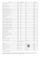
Program Memory Type: Flash
Program Memory Size (KB): 4
CPU Speed (MIPS/DMIPS): 20
SRAM Bytes: 256
Data
EEPROM ()/HEF (bytes): 256
Digital Communication Peripherals: 1-SPI, 1-I2C
Capture/Compare/PWM Peripherals: 1 Input Capture, 1 CCP, 4PWM
Timers: 1 x 8-bit, 1 x 16-bit
Number of Comparators: 1
Temperature Range (C): -40 to 85
Operating Voltage Range (V): 1.8 to 5.5
Pin Count: 14
Low Power: Yes
Table 1. The Flash memory structure []
Address Function Size (Bytes)
0x8000 - 0x80FF DNA 256
0x8100 - 0x817F Factory Calibration 128
0x8180 - 0x83FF Future use 896
The Zmod
ADC () is compliant with SYZYGY™ Specification (https://syzygyfpga.io/specification/). It contains an MCU able to calculate the
Geographical Address and provide the DNA information via I2C. The DNA is stored in the MCU FLASH at the address range: 0x8000 - 0x80FF with the
following structure:
Table 2. The Zmod ADC DNA structure []
V
in
= +
CA
(45)
N
⋅
Range
⋅ (1 +
CG
)
2
13
in
40
2.7 Scope Spectral Characteristics
Fig. 12 shows a typical spectral characteristic of the scope input stage. A PXIe-5433 80 MHz () Function/Arbitrary Waveform Generator was used to
generate the input signal of 0.9V, for High Gain Scale, respectively 10V for the Low Gain scale. A Tektronix DPO5204B scope was used for measuring the
reference signal (at the scope SMA connector) and the output signal (at the input of the ADC ()). A differential probe was used to read the output signal on
the pads of the unloaded C115. The signal swept from 800kHz to 80MHz. The effective values of the input and output signals were recorded for each
frequency. The measurements were furter processesd to display the input stage frequency characteristics, as shown in Fig. 10.
For both scales, the 3dB bandwidth is 70MHz+. The 0.5dB bandwidth is 30MHz and the 0.1dB bandwidth is 20MHz.
The standard -3dB bandwidth definition is derived from filter theory. At cutout frequency, the scope attenuates the spectral components by 0.707, assuming
an error of ~30%, way too high for a measuring instrument. The bandwidth with a specified flatness is useful to better define the scope spectral
performances. The Zmod ADC () exhibits 30MHz+ @ 0.5dB, meaning that a 30 MHz () sinusoidal signal is shown with a flatness error of a max 5.6%.
20MHz @ 0.1dB means that a 5 MHz () sinusoidal signal is shown with a flatness error of a max 1.1%.
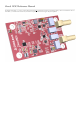
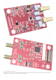
3. MCU
The
ATtinny44 MCU in Fig. 13 works as a I2C memory, storing the SYZYGY™ DNA information and the Calibration Coefficients. The J5 connector
is used for programming the MCU and the SYZYGY™ DNA at manufacturing.
The DNA and the Factory Calibration Coefficients are stored in the Flash memory of the MCU, which appears to the I2C interface as “read-only”. The
User Calibration Coefficients are stored in the EEPROM () memory of the MCU, which is write-protected via a magic number at a magic address. The
memory structure can be consulted below.
3.1. SYZYGY™ DNA