
User Manual


Heading 1
Name Size
(Bytes) Type
Flash Address (Factory
Calibration)
EEPROM () Address (User
Calibration)
Channel 2 HG
Offset
CA 4 float32 0x8124 0x7024
Channel 1
Linearity
34 uchar 0x8146 0x7046
Channel 2
Linearity
34 uchar 0x8168 0x7068
Log 22 string 0x817E 0x707E
CRC 1 uchar 0x817F 0x707F
Table 4. The EEPROM Memory Map []
Address Function Size (Bytes)
0x7000 - 0x707F User Calibration 128
0x7080 - 0x70FF Future Use 128
At the power up the
EEPROM () memory is protected against write operations. To disable the write protection one has to write a magic
number to a magic address over I2C. To re-enable the write protection one has to write a any other number to the magic address.
Table 5. The Write Protection Disable magic number and address []
Magic Number Magic Adress
0xD2 0x6FFF
This block includes the internal power supplies.
The Zmod
DAC () gets the digital rails from the carrier board, via the SYZYGY™ connector:
VCC5V0 - used for relays and analog supplies
VCC3V3 - used for the MCU and analog supplies
Vadj = 1.8V - used for the DAC () digital rail
The internal analog rails sequence is:
AVCC3V3 - DAC () analog rail, I/V converter (after VCC5V0)
AVCC-2V5 - I/V converter (after VCC5V0)
AVCC-8V0, AVCC8V0 - AWG output stage (after VCC3V3)
Input voltage supply range: 2.3 V to 5.5 V
300 mA maximum output current
Fixed and adjustable output voltage versions
Very low dropout voltage: 85 mV at 300 mA load
Low quiescent current: 45 µA at no load
Low shutdown current: <1 µA
Initial accuracy: ±1% accuracy
Up to 31 fixed-output voltage options available from 1.75 V to 3.3 V
4. Power Supplies
4.1. AVCC3V3
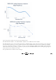
The analog supply AVCC3V3 is built from VCC5V0 using IC10, an
ADP122 5.5 V Input, 300 mA, Low Quiescent Current, CMOS
Linear Regulator, Fixed Output Voltage. To reduce noise in the I/V stage, the rail uses the LC filter: FB5 in Fig. 5.