
User Manual


Adjustable-output voltage range 0.8 V to 5.0 V (ADP123)
Excellent PSRR performance: 60 dB at 100
kHz ()
Excellent load/line transient response
Optimized for small 1.0 μF ceramic capacitors
Current limit and thermal overload protection
Logic controlled enable
Compact packages: 5-lead TSOT and 6-lead 2 mm × 2 mm LFCSP
1.2 A maximum load current
±2% output accuracy over temperature range
1.4
MHz () switching frequency
High efficiency up to 91%
Current-mode control architecture
Output voltage from 0.8 V to 0.85 × VIN
Automatic PFM/PWM mode switching
Integrated high-side MOSFET and bootstrap diode,
Internal compensation and soft start
Undervoltage lockout (UVLO), Overcurrent protection (OCP) and thermal shutdown (TSD)
Available in ultrasmall, 6-lead TSOT package
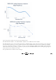
Figure 14. AVCC-2V5 []
The output voltage is:
Where:
Figure 13. AVCC3V3 []
4.2. AVCC-2V5
The AVCC-2V5 analog power supply is implemented with the
ADP2301 Step-Down regulator in an inverting Buck-Boost
configuration. See application Note
AN-1083: Designing an Inverting Buck Boost Using the ADP2300 and ADP2301 To reduce
noise and reduce the crosstalk between supplied circuits, the rail uses the LC filter: FB3 in Fig. 5.. The ADP2301 features:
V
OUT
= −
V
FB
⋅ = −2.5
V
(19)
R
49
+
R
50
R
50
V
FB
= 0.8
V typical
(20)
4.3. AVCC8V0