
User Manual
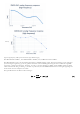


Figure 16. AVCC-8V0 []
The output voltage is:
Where:
The supply is enabled after VCC5V0 and AVCC3V3.
The SYZYGY™ connector in provides the interface with the carrier board. The used signals are:
Power rails
VCC5V0
VCC3V3
VADJ - needs to be set by the carier board to 1.8V
GND ()
Shield
SYZYGY™ I2C bus:
MCU_SCLUSCK
MCU_SDA_
MOSI ()
DAC () single ended input clock
CLKIN_AWG (coupled with
GND () in the differential C2P pair)
DAC () single ended output clock:
CLKIO_AWG (coupled with
GND () in the differential P2C pair)
R_GA for geographical address identification
Gain selector signals:
SET_FS_AWG1
V
A
V CC
8
V
0
= −
V
FB
⋅ = −8.035
V
(23)
R
56
R
60
V
FB
= 1.235
V typical
(24)
5. The SYZYGY™ Connector