
User Manual


The Analog Devices AD9717 dual, low-power 14-bit TxDAC digital-to-analog converter is used to generate the wave. The main
features are:
Power dissipation @ 3.3V, 2 mA output: 86 mW @ 125MS/s, sleep mode: <3 mW @ 3.3V
Supply voltage: 1.8V to 3.3V
SFDR to Nyquist: 84 dBc @ 1 MHz () output, 75 dBc @ 10 MHz () output
AD9717 NSD @ 1 MHz () output, 125MS/s, 2 mA: −151 dBc/Hz ()
Differential current outputs: 1 mA to 4 mA
CMOS inputs with single-port operation
Output common mode: 0 to 1.2 V
Small footprint, 40-lead LFCSP RoHS-compliant package
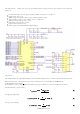
Figure 4. DAC. []
The parallel Data Bus, the single ended 100 MHz () clock and the SPI configuration bus are driven by the SYZYGY™ carrier board
FPGA. External V reference voltage is used. The Full Scale is set via the FSADJx pins. The ADG787
2.5Ω CMOS Low Power Dual 2:1
MUX/DEMUX is used to connect of either 8kΩ (for high gain) or 32kΩ (for low gain) from FSADJx pin to GND ().
The Full Scale DAC () output current is:
For high-
gain (High Range):
For low-gain (Low Range):
REFIO_AW
G
R
set
I
outAWGFS
= 32 ⋅ (2)
V
REFIO
_
AWG
R
set
I
outAWGFS
_
HG
= 32 ⋅ = 3.97
mA
(3)
1
V
8.06
k
Ω
I
outAWGFS
_
HG
= 32 ⋅ = 1
mA
(4)
1
V
32
k
Ω
The
ADG787 features: