
User Manual


Low noise: 2.1 nV/√Hz input voltage noise; 2.1 pA/√Hz input current noise
Custom compensation
Constant bandwidth from G = −1 to G = −10
High speed: 200
MHz () (G = −1), 190 MHz () (G = −10)
Low power: 34 mW or 6.7 mA typical for 5 V supply
Output disable feature, 1.3 mA
Low distortion: −93 dBc second harmonic, fC = 1 MHz (); −108 dBc third harmonic, fC = 1 MHz ()
DC precision: 1 mV maximum input offset voltage; 0.5 μV/°C input offset voltage drift
Wide supply range, 5 V to 24 V
Low price
Small packaging: Available in SOIC-8 and MSOP-8
The output voltage range depends on High-gain versus Low-gain selection:
Low-gain is used to generate low amplitude signals with improved accuracy. Any amplitude of the output signal can be generated by
combining LowGain/HighGain setting (rough) with the digital signal amplitude (fine).
With the 14-bit
DAC (), the absolute resolution of the AWG AC component is:
AD8021 is supplied with +8.5V/-8V (the VCC8V0 voltage is in fact 8.5V). Conform to the data sheet, the worst case output voltage
swing is V +1.8V to V -2.2V.
The nominal resistance of the PTC in the feedback loop is 33 ohm. The maximum current delivered by te AWG is 30mA.
To avoid saturation, the voltage in should stay in:
Only inner (tighter) ranges are used in equations and , for providing tolerance margins.
To generate a particular voltage value at the output of the AWG channel, the user application sends a signed 14 bit integer to the
DAC ().
This value is computed as:
were:
Vout = the desired output voltage. Could be separated in:
Voffset= the DC component voltage
Vamplitude= the AC instantaneous voltage
CA = calibration additive constant (for the appropriate channel and gain; see Table 3)
CG = calibration Gain constant (for the appropriate channel and gain; see Table 3)
Range = the ideal AWG output stage range (approximation of the values in equation ):
1 * 1.33 = 1.33 (for LG: +/-1.25V) or
4 * 1.33 = 5.32 (for HG: +/-5V)
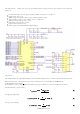
The R146 PTC thermistor provides thermal protection in case of an output short-circuit.
The IC7 relay (non-latching) is OPEN at the power-on, decoupling the power-on glitch of the OpAmp from the load. It is CLOSED by
the FPGA, via Q1. R37 is a pull down when IC7 is OPEN and a dummy load when IC7 is CLOSED. D2 is an ESD suppressor.
R36 is the 50Ω AWG output impedance.
2.4. AWG Out
IC8 in Fig. 5 is the output stage of the AWG. features:
V
AWG REL
=
V
OUT IC
5
B
⋅ (1 + ) = 5.51 ⋅
V
OUT IC
5
B
(9)
R
41
R
42
−5.49
V
< −5
V
<
V
AWG REL HG
< 5
V
< 5.45
V
−1.37
V
< 1.25
V
<
V
AWG REL LG
< 1.25
V
< 1.37
V
(10)
at Low Gain
: = 167
μV
2.74
V
2
14
at High Gain
: = 665
μV
(11)
10.9
V
2
14
- +
9
−8
V
+ 1.8
V
+ 33Ω ∗ 30
mA
= −5.21
V
< −5
V
<
V
AWG REL
< 5
V
< 8.5 − 2.2
V
− 33Ω ∗ 30
mA
= 5.31
V
(12)
10 12
N
= ∗ 2
13
∈ (−2
13
, +2
13
) (13)
(
V
Out
−
CA
)
(1 +
CG
) ⋅ (
Range
)
10