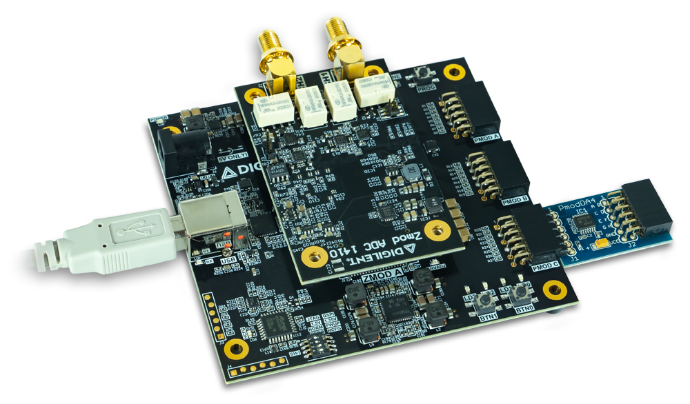
USB104 A7 Hardware Reference Manual The USB104 A7 conforms to the industry-standard PC/104 form factor, and brings power and versatility to your PC/104 stackable PC. It features an Xilinx Artix-7 XC7A100T. Artix®-7 devices provide the highest performance-per-watt fabric making the USB104 A7 ideal for size, weight, and power constrained projects. I/O is provided with three 12-pin Pmod ports, a SYZYGY-compatible Zmod port.
Features Xilinx Artix-7 FPGA (XC7A100T-1CSG324I) 15,850 slices containing four 6-input LUTs and 8 flip-flops apiece 4,860 Kbits of fast block RAM () 6 Clock Management Tiles (CMTs), each with a phase-locked loop and mixed-mode clock manager 240 DSP slices Internal clock speeds exceeding 450MHz On-chip analog-to-digital converter (XADC) for FPGA die temperature monitoring Programmable over JTAG and Quad-SPI Flash Memory 512 MB () Micron DDR3 with 16-bit bus @ 800 or 667 MT/s depending on configurable voltage
DNA interfaces connected to Platform MCU allowing for various auto-negotiated power supply configurations Pmod Ports 3 twelve-pin ports with a total of 24 FPGA-connected I/Os User GPIO () 2 push-buttons 4 LEDs USB104 A7 Callout Diagram Callout # Description Callout # Description Callout # Description 1 Xilinx Artix-7 FPGA 6 FPGA Programming Reset Button 10 Zmod/SYZYGY Port 2 Micron DDR3 Memory 7 Pmod Ports 11 Mode Select Switches 3 Barrel Jack for External Power Supply 8 User Buttons a
An overview of the power circuit is shown in Figure 1.1: Figure 1.1: Power Circuit Overview All on-board power supplies are automatically sequenced on when a power supply, whether USB or an external supply connected to the barrel jack (), is connected to the board. The power indicator LED (), labeled “LDP”, is illuminated (color) when all supply rails reach their nominal voltage.
Net Name Upstream Net Name Power IC Type Power IC Label Min/Typ/Max Voltage Max Current Major Devices and Connectors VCC1V0 VCC5V0 Buck IC14 1.0V +- 5% 2.5A FPGA VCC1V8 VCC5V0 Buck IC14 1.8V +- 5% 1.0A FPGA, USB JTAG/UART DDRVCC VCC5V0 Buck IC14 1.35V/1.5V1) +5% 2.0A FPGA, DDR3/DDR3L DDRVTT DDRVCC, VCC5V0 LDO IC11 0.675V/0.75V2) +- 5% 0.43A DDR3/DDR3L VCC3V3 VCC5V0 Buck IC17 3.3V +- 5% 3.
2. FPGA Configuration After power-on, the Artix-7 FPGA must be configured (or programmed) before it can perform any functions. The FPGA can be configured in one of two ways: 1. A PC can use the Digilent USB-JTAG circuitry connected to the USB port (J2, labeled “USB”), to program the FPGA any time the power is on. 2. A file stored in the nonvolatile serial (SPI) flash device can be transferred to the FPGA using the SPI port. Figure 2.1: USB104 A7 Configuration Options Figure 2.
3. DDR3/DDR3L Memory The USB104 A7 includes one MT41K256M16TW-107 memory component, creating a single rank, 16-bit wide interface with 512MB of capacity. It is routed to an HR (High Range) FPGA bank, powered at either 1.35V or 1.5V (discussed in Section 3.1, DDR3 Voltage Levels, below), with 40 ohm controlled single-ended trace impedance. 40 ohm internal terminations in the FPGA are used to match the trace characteristics.
Switch Position DDRVCC Voltage DDRVTT Voltage 1.5V (OFF) 1.5V 0.75V 1.35V (ON) 1.35V 0.675V 4. Quad-SPI Flash FPGA configuration files can be written to the Quad-SPI Flash (Spansion part number S25FL128SAGMF100), and setting the programming mode select switch (SW1/0) will cause the FPGA to automatically read a configuration from this device at power on. An Artix-7 100T configuration file requires 30,606,304 bits of memory, leaving about 76% of the flash device (or ~12MB) available for user data.
6. USB Port The USB104 A7 includes a high-retention USB-B port intended for all communication with a host computer. This port is connected to a USB hub which breaks out the traffic into several different FPGA-connected interfaces, via a FTDI FT2232HQ USB-UART bridge and a FTDI FT232H hi-speed single-channel USB to UART/FIFO bridge. The USB hub and the two controller are transparent to the user.
Signal Direction (FPGA) Description RD# Output A low pulse triggers data to be read out from the FIFO. WR# Output A low pulse triggers data to be written to the FIFO. SIWU# Output Send Immediate or Wake-up. In normal mode, a low pulse triggers sending a data packet with teh data currently in the FIFO, even if below the normal packet size. In suspend mode, a low pulse can wake up the host computer. OE# Output When low, the data bus is driven by the USB controller (read transfer).
Warning: SYZYGY pods are NOT hot-swappable. Connecting or disconnecting a pod from the USB104 A7 while the board is powered on may cause damage to the pod and/or the board, and is to be avoided. A SYZYGY Standard interface contains 16 single-ended I/O pins, 8 differential I/O pairs (which can alternatively be used as 16 additional single-ended I/O pins), and two dedicated differential clocks - one for input and one for output.
Table 8.1: USB104 A7 Pmod Pinout. Pmod JA Pmod JB Pmod JC Pmod Type Standard Standard Standard Pin 1 F4 C4 C5 Pin 2 F3 B2 C6 Pin 3 E2 B3 B6 Pin 4 D2 B4 C7 Pin 7 H2 B1 A5 Pin 8 G2 A1 A6 Pin 9 C2 A3 B7 Pin 10 C1 A4 D8 The standard Pmod connectors are connected to the FPGA via 200 Ohm series resistors. The series resistors prevent short circuits that can occur if the user accidentally drives a signal that is supposed to be used as an input.


