
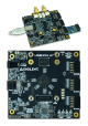
User Manual


Xilinx Artix-7 FPGA (XC7A100T-1CSG324I)
15,850 slices containing four 6-input LUTs and 8 flip-flops apiece
4,860 Kbits of fast block
RAM ()
6 Clock Management Tiles (CMTs), each with a phase-locked loop and mixed-mode clock manager
240 DSP slices
Internal clock speeds exceeding 450MHz
On-chip analog-to-digital converter (XADC) for FPGA die temperature monitoring
Programmable over JTAG and Quad-SPI Flash
Memory
512 MB () Micron DDR3 with 16-bit bus @ 800 or 667 MT/s depending on configurable voltage
16 MB () Spansion Quad-SPI Flash
Power
Powered over USB or 5V external power source
USB
DPTI/DSPI Data Transfer Interface
USB-JTAG Programming Circuitry
USB-UART Bridge
Zmod Port
One ports following the SYZYGY Standard interface specification
Compatible with a variety of SYZYGY pods, allowing for a wide variety of applications
Dedicated differential clocks for input and output
8 differential I/Os
16 single-ended I/Os
Features