
User Manual


1-Aug-2012
22
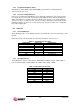
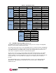
Table 15 – Ethernet PHY Pin Assignment and Definitions
Signal Name
Description
Zynq EPP pin
88E1510 pin
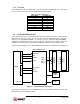
RX_CLK
Receive Clock
A14
40
RX_CTRL
Receive Control
D7
37
RXD[3:0]
Receive Data
RXD0: E11
RXD1: B7
RXD2: F12
RXD3: A13
38
39
41
42
TX_CLK
Transmit Clock
D6
47
TX_CTRL
Transmit Control
F11
2
TXD[3:0]
Transmit Data
TXD0: E9
TXD1: A7
TXD2: E10
TXD3: A8
44
45
48
1
MDIO
Management Data
C12
5
MDC
Management Clock
D10
4
The datasheet for the Marvell 88E1518 is not available publicly. An NDA is required for this
information. Please contact your local Avnet or Marvell representative for assistance.
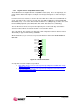
2.9 Expansion Headers
2.9.1 LPC FMC Connector
A single low-pin count (LPC) FMC slot is provided on the ZedBoard to support a large ecosystem
of plug-in modules. The LPC FMC exposes 68 single-ended I/O, which can be configured as 34
differential pairs. The FMC interface spans over two PL I/O banks, banks 34 and 35. To meet
the FMC spec, these banks are powered from an adjustable voltage set by jumper, J18.
Selectable voltages include 1.8V, default, and 2.5V. It is also possible to set Vadj to 3.3V. Since
3.3V could potentially be the most damaging voltage setting for Vadj, this is not available with the
default board hardware. To set Vadj to 3.3V, solder a short across the 3V3 pads at J18 or solder
in an additional 1x2 header.
WARNING: Before attaching a FMC Card, ensure the correct voltage is selected on jumper, J18.
Failure to do so may result in damage to the FMC card and/or the ZedBoard.
Note, the following LPC FMC connections guidelines were followed:
CLK_#_M2C
– 50 ohm single-ended impedance
– Less than 10mil skew in P/N pair
– Connected to GC (Global Clock) preferential or MRCC (Multi-Region) if not
available
– No length matching to any other feature
LA bus
– 50 ohm single-ended impedance
– Less than 10mil skew in P/N pair
– Less than 100mil length skew across all bits in a bus
• No restriction between LA, HA or HB
– LA Bus 0:16 to be located in one bank
– LA Bus 17:33 to be located in one bank
– CC Pairs 0, 17 to be placed on MRCC pins
– CC Pairs 1, 18 to be placed on SRCC pins
• HB_06_CC optional placed on clock pin if available
To conserve EPP pins, GA[1:0] were removed from EPP and connected to GND.