300 Henley Court Pullman, WA 99163 509.334.6306 www.digilent.com PYNQ-Z1 Board Reference Manual Revised April 13, 2017 Overview The PYNQ-Z1 board is designed to be used with PYNQ, a new open-source framework that enables embedded programmers to exploit the capabilities of Xilinx Zynq All Programmable SoCs (APSoCs) without having to design programmable logic circuits. Instead the APSoC is programmed using Python, with the code developed and tested directly on the PYNQ-Z1.
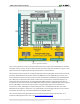
PYNQ-Z1 Board Reference Manual The PYNQ-Z1. Memory o 512MB DDR3 with 16-bit bus @ 1050Mbps o 16MB Quad-SPI Flash with factory programmed 48-bit globally unique EUI-48/64™ compatible identifier o microSD slot USB and Ethernet o Gigabit Ethernet PHY o USB-JTAG Programming circuitry o USB-UART bridge o USB OTG PHY (supports host only) Audio and Video o HDMI sink port (input) o HDMI source port (output) o Microphone with PDM interface o PWM driven mono audio output with 3.
PYNQ-Z1 Board Reference Manual A USB 2.0 port can deliver maximum 0.5A of current according to the specifications. This should provide enough power for lower complexity designs. More demanding applications, including any that drive multiple peripheral boards or other USB devices, might require more power than the USB port can provide. In this case, power consumption will increase until it’s limited by the USB host. This limit varies a lot between manufacturers of host computers and depends on many factors.
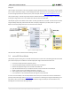
PYNQ-Z1 Board Reference Manual Figure 2.1. Zynq APSoC architecture. The PL is nearly identical to a Xilinx 7-series Artix FPGA, except that it contains several dedicated ports and buses that tightly couple it to the PS. The PL also does not contain the same configuration hardware as a typical 7-series FPGA, and it must be configured either directly by the processor or via the JTAG port.
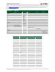
PYNQ-Z1 Board Reference Manual Table 2.1 depicts the external components connected to the MIO pins of the PYNQ-Z1. The Zynq Presets File found on the PYNQ-Z1 Resource Center can be imported into EDK and Vivado Designs to properly configure the PS to work with these peripherals. MIO 500 3.
PYNQ-Z1 Board Reference Manual MIO 501 1.8V Pin 39 40 41 42 43 44 45 46 47 48 (N/C) 49 (N/C) 50 (N/C) 51 (N/C) 52 Peripherals ENET 0 53 MDIO USB 0 DATA7 SDIO 0 CCLK CMD D0 D1 D2 D3 RESETN CD MDC Table 2.1. MIO Pinout. 3 Zynq Configuration Unlike Xilinx FPGA devices, APSoC devices such as the Zynq-7020 are designed around the processor, which acts as a master to the programmable logic fabric and all other on-chip peripherals in the processing system.
PYNQ-Z1 Board Reference Manual Stage 2 The last stage is the execution of the user application that was loaded by the FSBL. This can be any sort of program, from a simple “Hello World” design, to a Second Stage Boot loader used to boot an operating system like Linux. For a more thorough explanation of the boot process, refer to Chapter 6 of the Zynq Technical Reference manual. The Zynq Boot Image is created using Vivado and Xilinx Software Development Kit (Xilinx SDK).
PYNQ-Z1 Board Reference Manual 3.2 Quad SPI Boot Mode The PYNQ-Z1 has an onboard 16MB Quad-SPI Flash that the Zynq can boot from. Documentation available from Xilinx describes how to use Xilinx SDK to program a Zynq Boot Image into a Flash device attached to the Zynq. Once the Quad SPI Flash has been loaded with a Zynq Boot Image, the following steps can be followed to boot from it: 1. 2. 3. 3.3 Attach a power source to the PYNQ-Z1 and select it using JP5.
PYNQ-Z1 Board Reference Manual 5 DDR Memory The PYNQ-Z1 includes an IS43TR16256A-125KBL DDR3 memory components creating a single rank, 16-bit wide interface and a total of 512MiB of capacity. The DDR3 is connected to the hard memory controller in the Processor Subsystem (PS), as outlined in the Zynq documentation. The PS incorporates an AXI memory port interface, a DDR controller, the associated PHY, and a dedicated I/O bank. DDR3 memory interface speeds up to 533 MHz/1066 Mbps are supported.
PYNQ-Z1 Board Reference Manual The Zynq presets file (available in the PYNQ-Z1 Resource Center) takes care of mapping the correct MIO pins to the UART 0 controller and uses the following default protocol parameters: 115200 baud rate, 1 stop bit, no parity, 8-bit character length. Two on-board status LEDs provide visual feedback on traffic flowing through the port: the transmit LED(LD11) and the receive LED (LD10).
PYNQ-Z1 Board Reference Manual Figure 7.1. microSD slot signals. Both low speed and high speed cards are supported, the maximum clock frequency being 50 MHz. A Class 4 card or better is recommended. Refer to section 3.1 for information on how to boot from an SD card. For more information, consult the Zynq Technical Reference manual. 8 USB Host The PYNQ-Z1 implements one of the two available PS USB OTG interfaces on the Zynq device. A Microchip USB3320 USB 2.
PYNQ-Z1 Board Reference Manual 9 Ethernet PHY The PYNQ-Z1 uses a Realtek RTL8211E-VL PHY to implement a 10/100/1000 Ethernet port for network connection. The PHY connects to MIO Bank 501 (1.8V) and interfaces to the Zynq-7000 APSoC via RGMII for data and MDIO for management. The auxiliary interrupt (INTB) and reset (PHYRSTB) signals connect to MIO pins MIO10 and MIO9, respectively. Figure 9.1. Ethernet PHY signals.
PYNQ-Z1 Board Reference Manual Although the default power-up configuration of the PHY might be enough in most applications, the MDIO bus is available for management. The RTL8211E-VL is assigned the 5-bit address 00001 on the MDIO bus. With simple register read and write commands, status information can be read out or configuration changed. The Realtek PHY follows industry-standard register map for basic configuration.
PYNQ-Z1 Board Reference Manual Pin/Signal SCL, SDA HPD/HPA J11 (source) Description DDC bidirectional Hot-plug detect input (inverted) FPGA pin M17, M18 R19 J10 (sink) Description DDC bidirectional Hot-plug assert output FPGA pin U14, U15 T19 Table 10.1. HDMI pin description and assignment. 10.1 TMDS Signals HDMI/DVI is a high-speed digital video stream interface using transition-minimized differential signaling (TMDS).
PYNQ-Z1 Board Reference Manual Figure 11.1 outlines the clocking scheme used on the PYNQ-Z1. Note that the reference clock output from the Ethernet PHY is used as the 125 MHz reference clock to the PL, in order to cut the cost of including a dedicated oscillator for this purpose. Keep in mind that CLK125 will be disabled when the Ethernet PHY (IC1) is held in hardware reset by driving the PHYRSTB signal low. Figure 11.1. PYNQ-Z1 clocking.
PYNQ-Z1 Board Reference Manual 12.1 Tri-Color LEDs The PYNQ-Z1 board contains two tri-color LEDs. Each tri-color LED has three input signals that drive the cathodes of three smaller internal LEDs: one red, one blue, and one green. Driving the signal corresponding to one of these colors high will illuminate the internal LED. The input signals are driven by the Zynq PL through a transistor, which inverts the signals. Therefore, to light up the tri-color LED, the corresponding signals need to be driven high.
PYNQ-Z1 Board Reference Manual A PDM signal is generated from an analog signal through a process called delta-sigma modulation. A simple idealized circuit of delta-sigma modulator is shown in Figure 13.1.2. Figure 13.1.2. PDM Delta-Sigma Modulator. Sum Integrator Out Flip-flop Output 0.4-0=0.4 0.4-0=0.4 0.4-1=-0.6 0.4-0=0.4 0.4-1=-0.6 0.4-0=0.4 0.4-0=0.4 0.4-1=-0.6 0+0.4=0.4 0.4+0.4=0.8 0.8-0.6=0.2 0.2+0.4=0.6 0.6-0.6=0 0+0.4=0.4 0.4+0.4=0.8 0.8-0.6=0.2 0 1 0 1 0 0 1 0 Table 13.1.1.
PYNQ-Z1 Board Reference Manual The typical value of the clock frequency is 2.4 MHz. Assuming that the application requires 7-bit precision and 24 KHz, there can be two counters that count 128 samples at 12 KHz, as shown in Fig. 13.2.2. Figure 13.2.2. Example PDM Circuit. 14 Mono Audio Output The on-board audio jack (J13) is driven by a Sallen-Key Butterworth Low-pass 4th Order Filter that provides mono audio output. The circuit of the low-pass filter is shown in Fig. 14.1.
PYNQ-Z1 Board Reference Manual Figure 14.2. Audio Output Frequency Response. 14.1 Pulse-Width Modulation A pulse-width modulated (PWM) signal is a chain of pulses at some fixed frequency, with each pulse potentially having a different width.
PYNQ-Z1 Board Reference Manual Figure 14.1.2. PWM Output Voltage. 15 Reset Sources 15.1 Power-on Reset The Zynq PS supports external power-on reset signals. The power-on reset is the master reset of the entire chip. This signal resets every register in the device capable of being reset. The PYNQ-Z1 drives this signal from the PGOOD signal of the TPS65400 power regulator in order to hold the system in reset until all power supplies are valid. 15.
PYNQ-Z1 Board Reference Manual Digilent produces a large collection of Pmod accessory boards that can attach to the Pmod expansion connectors to add ready-made functions like A/D’s, D/A’s, motor drivers, sensors, and other functions. Each Pmod port found on Digilent FPGA boards falls into one of four categories: standard, MIO connected, XADC, or high-speed. The PYNQ-Z1 has two Pmod ports, both of which are the high-speed type. The following section describes the high-speed type of Pmod port. 16.
PYNQ-Z1 Board Reference Manual Figure 17.1. Shield Pin Diagram.
PYNQ-Z1 Board Reference Manual Pin Name Shield Function PYNQ-Z1 Connection XVREF XADC Analog Voltage Reference Connected to 1.25 V, 25mA rail used to drive the XADC voltage reference on the Zynq (VREFP) N/C Not Connected Not Connected IOREF Digital I/O Voltage reference Connected to the PYNQ-Z1 3.3V Power Rail (See the “Power Supplies” section) RST Reset to Shield Connected to the red “SRST” button and MIO pin 12 of the Zynq.
PYNQ-Z1 Board Reference Manual 17.2 Shield Analog I/O The pins labeled A0-A11 and V_P/V_N are used as analog inputs to the XADC module of the Zynq. The Zynq expects that the inputs range from 0-1 V. On the pins labeled A0-A5 we use an external circuit to scale down the input voltage from 3.3V. This circuit is shown in Fig. 17.2.1. This circuit allows the XADC module to accurately measure any voltage between 0V and 3.3V (relative to the PYNQ-Z1's GND) that is applied to any of these pins.
PYNQ-Z1 Board Reference Manual the FPGA. For more information on using the XADC core, refer to the Xilinx document titled “7 Series FPGAs and Zynq-7000 All Programmable SoC XADC Dual 12-Bit 1 MSPS Analog-to-Digital Converter”. It is also possible to access the XADC core directly using the PS, via the “PS-XADC” interface. This interface is described in full in chapter 30 of the Zynq Technical Reference manual. Copyright Digilent, Inc. All rights reserved.