
Data Sheet


PYNQ-Z1 Board Reference Manual
Copyright Digilent, Inc. All rights reserved.
Other product and company names mentioned may be trademarks of their respective owners.
Page 22 of 25
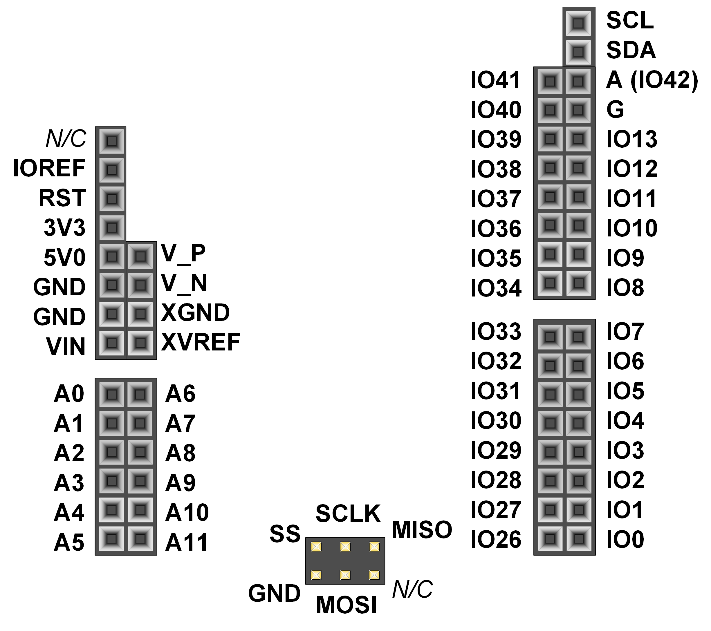
Figure 17.1. Shield Pin Diagram.
Pin Name
Shield Function
PYNQ-Z1 Connection
IO0-IO13, IO26-
IO41, A (IO42)
General purpose
I/O pins
See Section titled “Shield Digital I/O”
SCL
I2C Clock
See Section titled “Shield Digital I/O”
SDA
I2C Data
See Section titled “Shield Digital I/O”
SCLK
SPI Clock
See Section titled “Shield Digital I/O”
MOSI
SPI Data out
See Section titled “Shield Digital I/O”
MISO
SPI Data in
See Section titled “Shield Digital I/O”
SS
SPI Slave Select
See Section titled “Shield Digital I/O”
A0-A5
Single-Ended
Analog Input
See Section titled “Shield Analog I/O”
A6-A11
Differential Analog
Input
See Section titled “Shield Analog I/O”
V_P, V_N
Dedicated
Differential Analog
Input
See Section titled “Shield Analog I/O”
XGND
XADC Analog
Ground
Connected to net used to drive the XADC ground reference
on the Zynq (VREFN)