
Data Sheet


PYNQ-Z1 Board Reference Manual
Copyright Digilent, Inc. All rights reserved.
Other product and company names mentioned may be trademarks of their respective owners.
Page 24 of 25
17.2 Shield Analog I/O
The pins labeled A0-A11 and V_P/V_N are used as analog inputs to the XADC module of the Zynq. The Zynq
expects that the inputs range from 0-1 V. On the pins labeled A0-A5 we use an external circuit to scale down the
input voltage from 3.3V. This circuit is shown in Fig. 17.2.1. This circuit allows the XADC module to accurately
measure any voltage between 0V and 3.3V (relative to the PYNQ-Z1's GND) that is applied to any of these pins. If
you wish to use the pins labeled A0-A5 as Digital inputs or outputs, they are also connected directly to the Zynq PL
before the resistor divider circuit (also shown in Fig. 17.2.1).
Figure 17.2.1. Single-Ended Analog Inputs.
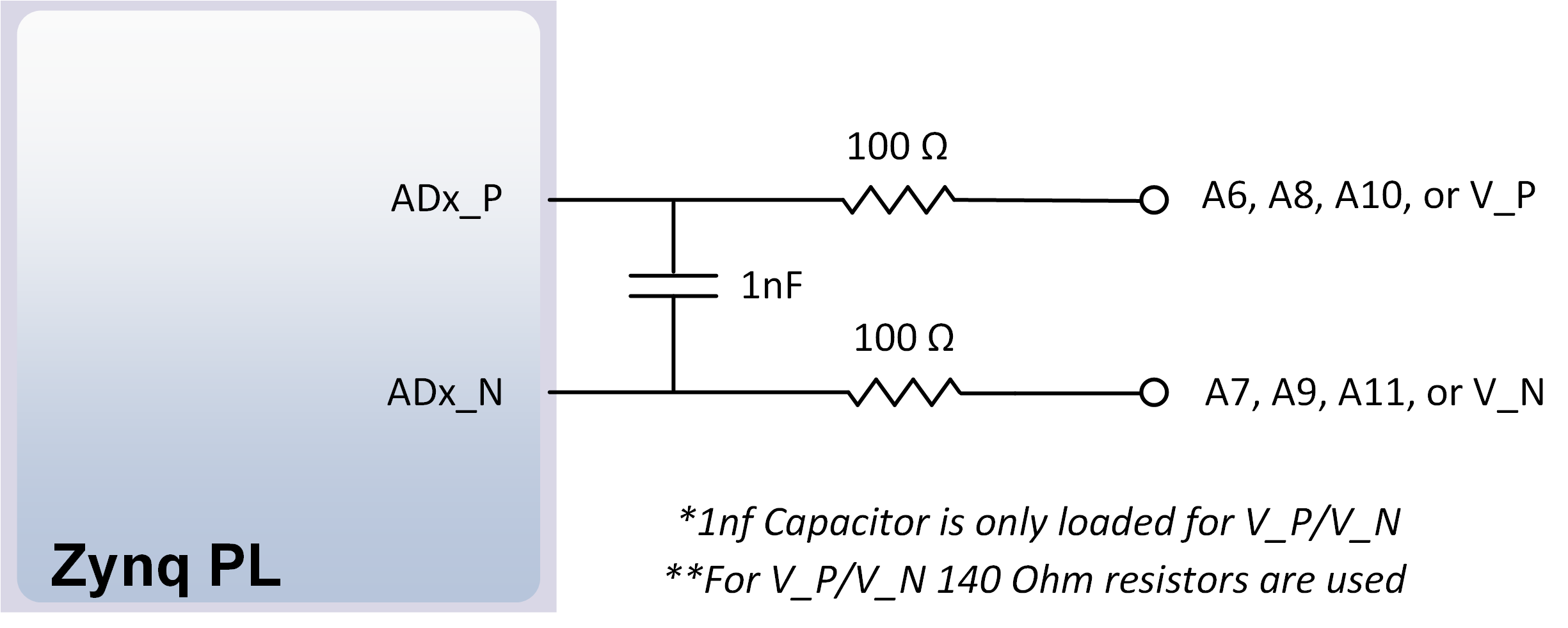
The pins labeled A6-A11 are connected directly to 3 pairs of analog capable pins on the Zynq PL via an anti-aliasing
filter. This circuit is shown in Fig. 17.2.2. These pairs of pins can be used as differential analog inputs with a voltage
difference between 0-1V. The even numbers are connected to the positive pins of the pair and the odd numbers
are connected to the negative pins (so A6 and A7 form an analog input pair with A6 being positive and A7 being
negative). Note that though the pads for the capacitor are present, they are not loaded for these pins. Since the
analog capable pins of the FPGA can also be used like normal digital FPGA pins, it is also possible to use these pins
for Digital I/O.
The pins labeled V_P and V_N are connected to the VP_0 and VN_0 dedicated analog inputs of the FPGA. This pair
of pins can also be used as a differential analog input with voltage between 0-1V, but they cannot be used as
Digital I/O. The capacitor in the circuit shown in Fig. 17.2.2 for this pair of pins is loaded on the PYNQ-Z1.
Figure 17.2.2. Differential Analog Inputs.
The XADC core within the Zynq is a dual channel 12-bit analog-to-digital converter capable of operating at 1 MSPS.
Either channel can be driven by any of the analog inputs connected to the shield pins. The XADC core is controlled
and accessed from a user design via the Dynamic Reconfiguration Port (DRP). The DRP also provides access to
voltage monitors that are present on each of the FPGA’s power rails, and a temperature sensor that is internal to