
Data Sheet


PYNQ-Z1 Board Reference Manual
Copyright Digilent, Inc. All rights reserved.
Other product and company names mentioned may be trademarks of their respective owners.
Page 9 of 25
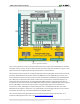
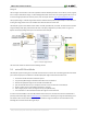
5 DDR Memory
The PYNQ-Z1 includes an IS43TR16256A-125KBL DDR3 memory components creating a single rank, 16-bit wide
interface and a total of 512MiB of capacity. The DDR3 is connected to the hard memory controller in the Processor
Subsystem (PS), as outlined in the Zynq documentation.
The PS incorporates an AXI memory port interface, a DDR controller, the associated PHY, and a dedicated I/O bank.
DDR3 memory interface speeds up to 533 MHz/1066 Mbps are supported.
1
PYNQ-Z1 was routed with 40 ohm (+/-10%) trace impedance for single-ended signals, and differential clock and
strobes set to 80 ohms (+/-10%). A feature called DCI (Digitally Controlled Impedance) is used to match the drive
strength and termination impedance of the PS pins to the trace impedance. On the memory side, each chip
calibrates its on-die termination and drive strength using a 240-ohm resistor on the ZQ pin.
Due to layout reasons, the two data byte groups (DQ[0-7], DQ[8-15]) were swapped. To the same effect, the data
bits inside byte groups were swapped as well. These changes are transparent to the user. During the whole design
process the Xilinx PCB guidelines were followed.
Both the memory chips and the PS DDR bank are powered from the 1.5V supply. The mid-point reference of 0.75V
is created with a simple resistor divider and is available to the Zynq as external reference.
For proper operation, it is essential that the PS memory controller is configured properly. Settings range from the
actual memory flavor to the board trace delays. For your convenience, the Zynq presets file for the PYNQ-Z1 is
provided on the resource center and automatically configures the Zynq Processing System IP core with the correct
parameters.
For best DDR3 performance, DRAM training is enabled for write leveling, read gate, and read data eye options in
the PS Configuration Tool in Xilinx tools. Training is done dynamically by the controller to account for board delays,
process variations and thermal drift. Optimum starting values for the training process are the board delays
(propagation delays) for certain memory signals.
Board delays are specified for each of the byte groups. These parameters are board-specific and were calculated
from the PCB trace length reports. The DQS to CLK Delay and Board Delay values are calculated specific to the
PYNQ-Z1 memory interface PCB design.
For more details on memory controller operation, refer to the Xilinx Zynq Technical Reference manual.
6 USB UART Bridge (Serial Port)
The PYNQ-Z1 includes an FTDI FT2232HQ USB-UART bridge (attached to connector J14) that lets you use PC
applications to communicate with the board using standard COM port commands (or the tty interface in Linux).
Drivers are automatically installed in Windows and newer versions of Linux. Serial port data is exchanged with the
Zynq using a two-wire serial port (TXD/RXD). After the drivers are installed, I/O commands can be used from the PC
directed to the COM port to produce serial data traffic on the Zynq pins. The port is tied to PS (MIO) pins and can
be used in combination with the UART 0 controller.
1
Maximum actual clock frequency is 525 MHz on the PYNQ-Z1 due to PLL limitation.