
Datasheet

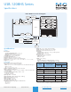

Table Of Contents

Measurement Computing (508) 946-5100
3
info@mccdaq.com mccdaq.com
USB-1208HS Series
T
rigger
A
/
D C
l
oc
k
In
A
/
D C
l
oc
k
Out
D/
A Clock In
D
/
A C
l
oc
k
Out
Cou
n
te
r In
0
Cou
n
te
r In 1
Tim
e
r
Out
13-bit 1 MS
8-channel A/D
Mux
A/D
PGA
FPGA
DIO
Protection
8
Data
Bus
Microcontroller with
High-Speed
USB 2.0
Compliant Interface
FIFO
Bus
Clock
EEPROM
USB
D+/D-
Power
Supplies
+16.5 V
- 16.5 V
1.2 V
3.3 V
5 V
VBUS
(5 V)
3.3 V
Always On
ENABLEs
Bitwise
Programmable
DIO
DIO
Protection
8
Bitwise
Programmable
DIO
12-bit dual D/A
DAC7553
Amp
D/A
Registers
D/A
Amp
12-bit dual D/A
DAC7553
Amp
D/A
Registers
D/A
Amp
SPI
SPI
SPI
8
2.5625 V
Reference
5.125 V
Reference
5.40 V Supply
USB-1208HS-2AO (2 DACs) and
USB-1208HS-4AO (4 DACs) only
USB-1208HS Series Block Diagram
Specifications
Specifications
General
Environment
Operating temperature range: 0 °C to 50 °C
Storage temperature range: –40 °C to 85 °C
Humidity: 0% to 90% non‑condensing
Communications: USB 2.0 (high‑speed)
Acquisition data buffer: 4 kS
Vibration: MIL STD 810E Category 1 and 10
Signal I/O connector: 2 banks of screw‑terminal blocks
Dimensions (L × W × H): 127.00 × 88.90 × 35.56 mm (5.00 × 3.50 × 1.40 in.)
Weight: 431 g (0.95 lb)
Analog Input
A/D converter: Successive approximation type
Input ranges: Software‑selectable per channel
DIFF: ±20 V, ±10 V, ±5 V (the voltage level on each individual AIN input is
limited to ±14 V.)
SE: ±10 V, ±5 V, ±2.5 V, 0 – 10 V
Number of channels: 4 DIFF/8 SE (software‑selectable)
Input configuration: Multiplexed
Channel gain queue: 8 unique consecutive elements, software‑selectable range
for each channel
Absolute maximum input voltage: CHx IN to GND
Power on: ±25 V max
Power off: ±12 V max
Input impedance: 35 MΩ min
Input bandwidth (–3 dB): All input ranges, 2 MHz typ
Input leakage current: ±250 nA typ
Input capacitance: 32 pf typ
Offset error drift: 5 ppm/°C typ
Gain error drift: 25 ppm/°C typ
Maximum working voltage (signal + common mode)
±20 V: ±14 V
±10 V: ±11 V
±5 V: ±5.5 V
Sample rate: 1 S/s to 1 MS/s, software‑selectable
Sample clock source: Internal A/D clock or AICKI
Burst mode: Software‑selectable, burst rate = 1 µs
Throughput
Software-paced: 33 S/s to 4000 S/s typ, system‑dependent
Hardware-paced: 1 MS/s max
Resolution: 13 bits
A/D no missing codes (uncalibrated)
DIFF mode: 13 bits
SE mode: 12 bits
CMRR: 60 Hz, 74 dB typ
Crosstalk
SE mode (all ranges, 250 kHz input signal): –62 dB typ
DIFF mode (all ranges, 250 kHz input signal): –78 dB typ
Voltage
Range
Calibrated Absolute
Accuracy (LSB)
Noise Performance*
Typical
Counts
LSBrms
DIFF mode
±20 V ±9.55 typ, ±13.18 max 3 0.45
±10 V ±4.59 typ, ±6.23 max 3 0.45
±5 V ±2.25 typ, ±2.75 max 3 0.45
SE mode
±10 V ±5.10 typ, ±8.06 max 5 0.91
±5 V ±2.63 typ, ±4.03 max 5 0.91
±2.5 V ±1.59 typ, ±2.70 max 5 0.91
0 V to 10 V ±3.29 typ, ±5.13 max 5 0.91
* Noise distribution is determined by gathering 50 kS with inputs tied to ground
at the user connector. Samples are gathered at the max rate of 1 MS/s.