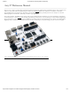
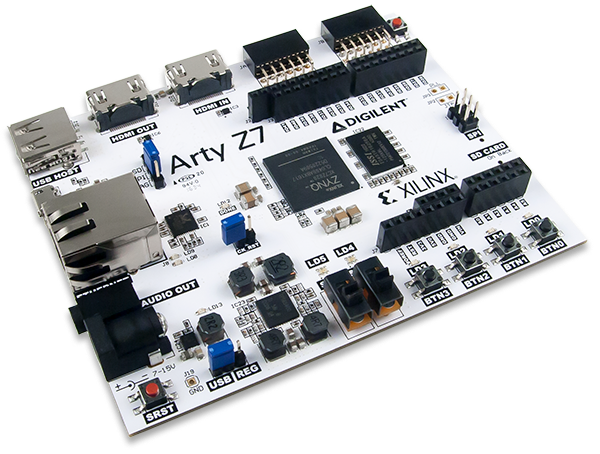
3/8/2018 Arty Z7 Reference Manual [Reference.Digilentinc] Arty Z7 Reference Manual The Arty Z7 is a ready-to-use development platform designed around the Zynq-7000™ All Programmable System-on-Chip (AP SoC) from Xilinx. The Zynq-7000 architecture tightly integrates a dual-core, 650 MHz () ARM Cortex-A9 processor with Xilinx 7-series Field Programmable Gate Array (FPGA) logic.
3/8/2018 Arty Z7 Reference Manual [Reference.Digilentinc] https://reference.digilentinc.
/8/2018 Arty Z7 Reference Manual [Reference.Digilentinc] Download This Reference Manual This reference manual not yet available for download. Features ZYNQ Processor 650MHz dual-core Cortex-A9 processor DDR3 memory controller with 8 DMA channels and 4 High Performance AXI3 Slave ports High-bandwidth peripheral controllers: 1G Ethernet, USB 2.
3/8/2018 Arty Z7 Reference Manual [Reference.Digilentinc] Expansion Connectors Two Pmod ports 16 Total FPGA I/O Arduino/chipKIT Shield connector Up to 49 Total FPGA I/O (see table below) 6 Single-ended 0-3.3V Analog inputs to XADC 4 Differential 0-1.0V Analog inputs to XADC Purchasing Options The Arty Z7 can be purchased with either a Zynq-7010 or Zynq-7020 loaded. These two Arty Z7 product variants are referred to as the Arty Z7-10 and Arty Z7-20, respectively.
3/8/2018 Arty Z7 Reference Manual [Reference.Digilentinc] The Arty Z7 is fully compatible with Xilinx’s high-performance Vivado Design Suite. This toolset melds FPGA logic design and embedded ARM software development into an easy to use, intuitive design flow. It can be used for designing systems of any complexity, from a complete operating system running multiple server applications in tandem, down to a simple bare-metal program that controls some LEDs.
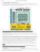
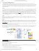
3/8/2018 Arty Z7 Reference Manual [Reference.Digilentinc] 2 Zynq APSoC Architecture The Zynq APSoC is divided into two distinct subsystems: The Processing System (PS) and the Programmable Logic (PL). Figure 2.1 shows an overview of the Zynq APSoC architecture, with the PS colored light green and the PL in yellow. Note that the PCIe Gen2 controller and Multi-gigabit transceivers are not available on the Zynq-7020 or Zynq-7010 devices. (https://reference.digilentinc.com/_detail/zybo/zyng1.
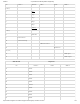
3/8/2018 Arty Z7 Reference Manual [Reference.Digilentinc] Pin ENET 0 SPI Flash USB 0 Shield UART 0 0 (N/C) 1 CS () 2 DQ0 3 DQ1 4 DQ2 5 DQ3 6 SCLK () 7 (N/C) 8 SLCK FB 9 Ethernet Reset 10 Ethernet Interrupt 11 USB Over Current 12 Shield Reset 13 (N/C) 14 UART Input 15 UART Output MIO 501 1.8V Peripherals Pin ENET 0 16 TXCK 17 TXD0 18 TXD1 19 TXD2 20 TXD3 21 TXCTL 22 RXCK 23 RXD0 24 RXD1 25 RXD2 https://reference.digilentinc.
3/8/2018 Arty Z7 Reference Manual [Reference.Digilentinc] 26 RXD3 27 RXCTL 28 DATA4 29 DIR 30 STP 31 NXT 32 DATA0 33 DATA1 34 DATA2 35 DATA3 36 CLK 37 DATA5 38 DATA6 39 DATA7 40 CCLK 41 CMD 42 D0 43 D1 44 D2 45 D3 46 RESETN 47 CD 48 (N/C) 49 (N/C) 50 (N/C) 51 (N/C) 52 MDC 53 MDIO Table 2.1. MIO Pinout https://reference.digilentinc.
3/8/2018 Arty Z7 Reference Manual [Reference.Digilentinc] 3 Zynq Configuration Unlike Xilinx FPGA devices, APSoC devices such as the Zynq-7020 are designed around the processor, which acts as a master to the programmable logic fabric and all other on-chip peripherals in the processing system. This causes the Zynq boot process to be more similar to that of a microcontroller than an FPGA.
3/8/2018 3. 4. 5. 6. 7. Arty Z7 Reference Manual [Reference.Digilentinc] Rename the Zynq Boot Image on the microSD card to BOOT.bin. Eject the microSD card from your computer and insert it into connector J9 on the Arty Z7. Attach a power source to the Arty Z7 and select it using JP5. Place a single jumper on JP4, shorting the two top pins (labeled “SD”). Turn the board on. The board will now boot the image on the microSD card. 3.
3/8/2018 Arty Z7 Reference Manual [Reference.Digilentinc] Both the memory chips and the PS DDR bank are powered from the 1.5V supply. The mid-point reference of 0.75V is created with a simple resistor divider and is available to the Zynq as external reference. For proper operation it is essential that the PS memory controller is configured properly. Settings range from the actual memory flavor to the board trace delays.
3/8/2018 Arty Z7 Reference Manual [Reference.Digilentinc] SD_CCLK Clock MIO40 5 SD_CMD Command MIO41 3 SD_CD Card Detect MIO47 9 Table 7.1. microSD pinout The SD slot is a powered from 3.3V, but is connected through MIO Bank 1/501 (1.8V). Therefore, a TI TXS02612 level shifter performs this translation. The TXS02612 is actually 2-port SDIO port expander, but only its level shifter function is used. The connection diagram can be seen on Figure 7.1.
3/8/2018 Arty Z7 Reference Manual [Reference.Digilentinc] The Arty Z7 uses a Realtek RTL8211E-VL PHY to implement a 10/100/1000 Ethernet port for network connection. The PHY connects to MIO Bank 501 (1.8V) and interfaces to the Zynq-7000 APSoC via RGMII for data and MDIO for management. The auxiliary interrupt (INTB) and reset (PHYRSTB) signals connect to MIO pins MIO10 and MIO9, respectively. (https://reference.digilentinc.com/_detail/reference/programmable-logic/arty-z7/arty-z7-eth.
3/8/2018 Arty Z7 Reference Manual [Reference.Digilentinc] The RGMII specification calls for the receive (RXC) and transmit clock (TXC) to be delayed relative to the data signals (RXD[0:3], RXCTL and TXD[0:3], TXCTL). Xilinx PCB guidelines also require this delay to be added. The RTL8211E-VL is capable of inserting a 2ns delay on both the TXC and RXC so that board traces do not need to be made longer. The PHY is clocked from the same 50 MHz () oscillator that clocks the Zynq PS.
3/8/2018 Arty Z7 Reference Manual [Reference.Digilentinc] HDMI/DVI is a high-speed digital video stream interface using transition-minimized differential signaling (TMDS). To make proper use of either of the HDMI ports, a standard-compliant transmitter or receiver needs to be implemented in the Zynq PL. The implementation details are outside the scope of this manual. Check out the vivado-library IP Core repository on the Digilent github (https://github.com/Digilent) for ready-to-use reference IP. 10.
3/8/2018 Arty Z7 Reference Manual [Reference.Digilentinc] The Arty Z7 board includes two tri-color LEDs, 2 switches, 4 push buttons, and 4 individual LEDs as shown in Figure 12.1. The push buttons and slide switches are connected to the Zynq PL via series resistors to prevent damage from inadvertent short circuits (a short circuit could occur if an FPGA pin assigned to a push button or slide switch was inadvertently defined as an output).
3/8/2018 Arty Z7 Reference Manual [Reference.Digilentinc] (https://reference.digilentinc.com/_detail/reference/programmable-logic/arty-z7/arty-z7-audio-sch.png?id=reference%3Aprogrammable-logic%3Aartyz7%3Areference-manual) Figure 13.1. Audio Output Circuit. The Audio shut-down signal (AUD_SD) is used to mute the audio output. It is connected to Zynq PL pin T17. To use the audio output, this signal must be driven to logic high.
3/8/2018 Arty Z7 Reference Manual [Reference.Digilentinc] (https://reference.digilentinc.com/_detail/reference/programmable-logic/arty-z7/arty-z7-audio-pdm.png?id=reference%3Aprogrammable-logic%3Aartyz7%3Areference-manual) Figure 13.1.1. PWM Waveform. The PWM signal must be integrated to define an analog voltage. The low-pass filter 3dB frequency should be an order of magnitude lower than the PWM frequency, so that signal energy at the PWM frequency is filtered from the signal.
3/8/2018 Arty Z7 Reference Manual [Reference.Digilentinc] (https://reference.digilentinc.com/_detail/reference/programmable-logic/arty-z7/arty-z7-pmod.png?id=reference%3Aprogrammable-logic%3Aartyz7%3Areference-manual) Figure 15.1. Pmod Port Diagram Digilent produces a large collection of Pmod accessory boards that can attach to the Pmod expansion connectors to add ready-made functions like A/D’s, D/A’s, motor drivers, sensors, and other functions. See www.digilentinc.com (http://www.digilentinc.
3/8/2018 Arty Z7 Reference Manual [Reference.Digilentinc] (https://reference.digilentinc.com/_media/reference/programmable-logic/arty-z7/arty-z7-shield.png) Figure 16.1. Shield Pin Diagram.
3/8/2018 Arty Z7 Reference Manual [Reference.Digilentinc] Pin Name Shield Function Arty Z7 Connection V_P, V_N Dedicated Differential Analog Input See Section titled “Shield Analog I/O” XGND XADC Analog Ground Connected to net used to drive the XADC ground reference on the Zynq (VREFN) XVREF XADC Analog Voltage Reference Connected to 1.
3/8/2018 Arty Z7 Reference Manual [Reference.Digilentinc] (https://reference.digilentinc.com/_media/reference/programmable-logic/arty-z7/arty-z7-shield-an.png) Figure 16.2.1. Single-Ended Analog Inputs. The pins labeled A6-A11 are connected directly to 3 pairs of analog capable pins on the Zynq PL via an anti-aliasing filter. This circuit is shown in Figure 16.2.2. These pairs of pins can be used as differential analog inputs with a voltage difference between 0-1V.
3/8/2018 Arty Z7 Reference Manual [Reference.Digilentinc] Last Name Email Address Submit Our Partners Xilinx University Program Help Customer Info Technical Support Forum Videos Company Info About Us (https://youtube.com/user/digilentinc)(https://store.digilentinc.com/p (https://store.digilentinc.com/partners/xilinx(https://forum.digilentinc.com) FAQ pageid=26) university-program/) Reference Wiki (https://resource.digilentinc.com/verify/faq) Shipping & Returns (https://reference.digilentinc.
3/8/2018 Arty Z7 Reference Manual [Reference.Digilentinc] (https://www.reddit.com/r/digilent) (https://www.linkedin.com/company/1454013) (https://www.flickr.com/photos/127815101@N07) https://reference.digilentinc.

