
Specifications


DAC1006/1007/1008—Simple Hookup for a “Quick Look” (Continued)
Settling Time: Settling time is the time required from a code
transition until the DAC output reaches within
±
1
⁄
2
LSB of the
final output value. Full-scale settling time requires a zero to
full-scale or full-scale to zero output change.
Full-Scale Error: Full scale error is a measure of the output
error between an ideal DAC and the actual device output.
Ideally, for the DAC1006 series, full-scale is V
REF
−1 LSB.
For V
REF
=
−10V and unipolar operation,
V
FULL-SCALE
=
10.0000V −9.8mV
=
9.9902V. Full-scale error is
adjustable to zero.
Monotonicity: If the output of a DAC increases for increas-
ing digital input code, then the DAC is monotonic. A 10-bit
DAC with 10-bit monotonicity will produce an increasing ana-
log output when all 10 digital inputs are exercised. A 10-bit
DAC with 9-bit monotonicity will be monotonic when only the
most significant 9 bits are exercised. Similarly, 8-bit monoto-
nicity is guaranteed when only the most significant 8 bits are
exercised.
2.0 DOUBLE BUFFERING
These DACs are double-buffered, microprocessor compat-
ible versions of the DAC1020 10-bit multiplying DAC. The
addition of the buffers for the digital input data not only al-
lows for storage of this data, but also provides a way to as-
semble the 10-bit input data word from two write cycles when
using an 8-bit data bus. Thus, the next data update for the
DAC output can be made with the complete new set of 10-bit
data. Further, the double buffering allows many DACs in a
system to store current data and also the next data. The up-
dating of the new data for each DAC is also not time critical.
When all DACs are updated, a common strobe signal can
then be used to cause all DACs to switch to their new analog
output levels.
3.0 TTL COMPATIBLE LOGIC INPUTS
To guarantee TTL voltage compatibility of the logic inputs, a
novel bipolar (NPN) regulator circuit is used. This makes the
input logic thresholds equal to the forward drop of two diodes
(and also matches the temperature variation) as occurs
naturally in TTL. The basic circuit is shown in
Figure 1
.A
curve of digital input threshold as a function of power supply
voltage is shown in the Typical Performance Characteristics
section.
4.0 APPLICATION HINTS
The DC stability of the V
REF
source is the most important
factor to maintain accuracy of the DAC over time and tem-
perature changes. A good single point ground for the analog
signals is next in importance.
These MICRO-DAC converters are CMOS products and rea-
sonable care should be exercised in handling them prior to fi-
nal mounting on a PC board. The digital inputs are protected,
but permanent damage may occur if the part is subjected to
high electrostatic fields. Store unused parts in conductive
foam or anti-static rails.
4.1 Power Supply Sequencing & Decoupling
Some IC amplifiers draw excessive current from the Analog
inputs to V− when the supplies are first turned on. To prevent
damage to the DAC — an external Schottky diode con-
nected from I
OUT1
or I
OUT2
to ground may be required to pre-
vent destructive currents in I
OUT1
or I
OUT2
. If an LM741 or
LF356 is used — these diodes are not required.
The standard power supply decoupling capacitors which are
used for the op amp are adequate for the DAC.
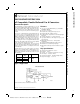
a. End Point Test After Zero and FS Adj.
DS005688-37
b. Best Straight Line
DS005688-38
www.national.com 8
PrintDate=1998/11/17 PrintTime=11:38:08 46711 ds005688 Rev. No. 4 cmserv Proof 8