ADVANCED DIGITAL MOLTI SlAVE Product Reference Manual ADVANCED DIGITAL CORPORATION USA OFFICE UNITED KINGDOM OFFICE 5432 PRODUCTION DRIVE HUNTINGTON BEACH. CA 92649 TELEPHONE: (714) 891...004 TELEX: 183210 ADVANCED HTBH 27 PRINCESS STREET HANOVER SQUARE.
MULTI SLAVE PRODUCT REFERENCE MANUAL Revision A.O Advanced Digital Corporation 5432 Production Drive Huntington Beach, Cali£ornia 92649 USA Telephone: (714) 891-4004 Telex: 183210 ADVANCED HTBH Advanced Digitsl (U.K.> Ltd. 27 Princess Street Hanover· Square London, U.K.
Copyright (C) 1985 by Advanced Digital Corporation 5432 Production Drive Huntington Beach, Cali£ornia 92649 All rights reserved. No part o£ this publication may be reproduced, transmitted, stored in a retrieval system, or translated into any language or computer language, in any £ora or by any means, electronic, mechanical, magnetic, optical, che~ical, Dsnual, or otherwise, without the prior written perMission o£ Advanced Digital Corporation.
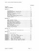
Multi Slave Product Reference Manual CONTENTS NOTICES TABLE OF CONTENTS ii SECTION I 1-1 i Introduction •••••••••••••••••••••••••••••••••••••• 1-1 Unpacking/Packing Instructions ••••••••••••••••.••• 1-1 Installation •••••••••••••••••••••••••••.•••••••••• 1-1 Warranty and Return Procedure ••••••••••••••••••••• 1-2 Features end Options •••••••••••••••••••••••••••••• 1-3 Functional Flow ••••••••••••••••••••••••.•••••••••• 1-4 Multi Slave Product Speci£ication •••••••••.••.
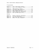
Multi Slave Product Reference Manual Illustrations: Figure 1-1 Figure 1-2 Multi Slave Block Diagrsn •••••.••.••••..•• 1-4 Multi Slave Component Layout •••••••••••.•• 1-6 2-1 2-2 2-3 2-4 2-5 2-6 PROM Selection Ju.per.s ..••.•••..•..••••.•. 2-2 Interrupt Jumper Selection ••••..••••••.••. 2-2 Base Address Selection .••••••••••••.••.••• 2-3 Master Status Port De£initions .••••••••••• 2-4 Slave Status Port De£initions •. 2-4 Bank and PROM Select Port .••••.
SECTION I
Multi Slave Product Reference Manual Section 1 INTRODUCTION This Product Re£erence Manual provides information to install, utilize and maintain the Advanced Digital Corp.'s Multi Slave S100 bus compatible computer. The Multi Slave is a single printed circuit board, conforming to the IEEE-696 form factor of 5.25 inches by 10 inches (13.33 cm by 25.4 cm), providing three independent 8 MHz 280 central processors, each with two 64k byte banks of memory, two serial 110 ports, and a counter/tiger.
Multi Slave Product Reference Manual Section 1 WARRANTY AND WARRANTY RETURN PROCEDURE Advanced Digital Corporation warrants that its products will be £ree from defects in material and workaanship £or a period of 360 days of shipment from the factory. 1£ a customer experiences a defect in either workManship or materials during the warranty period, noti£y your supplier i.mediately. Your supplier may repair the Multi Slave or deter.ine if some other action is'to be taken.
Multi Slave Product Reference Manual Section 1 FEATURES AND OPTIONS The Hulti Slave provides the following features: a Three independent a-bit, a MHz a Each CPU has 128k of memory, configured as two 64k byte banks, with a 1k to 16k area of co~~on (shared) memory. a Two asynchronous serial 110 ports per CPU. Level conversion to EIA RS-232C or RS-422 standards i& provided via the PS/NET (paddle card) accessory.
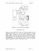
Multi Sleve Product Reference Manual Section 1 ..... .... ~ .. po' rt .. .... ~ ~ .. .--+ A +2681 DUARl ----. f4- -fJ r-- ... ... .... . ... PROM .1 Z80-H CPU (1 of 3) . ~ >--- .... r-----. ... Bank 64k RAM Control & Timing '-- p,r ~ L_---.. .. I NTER- FACE .... S-100 BUS "- Figura 1-1 Mult! Slave Block D1agraa FUNCTIONAL FLOW Figure 1-1 illustrates the maJor £unctionsl components of the Multi Slave computer board. Initially.
Multi Slave Product Re£erence Manual Section 1 HULTI SLAVE PRODUCT SPECIFICATIOH Physical and Environmental: For. Factor IEEE-696 S-100 standard 5.25 inches x 10.0 inches x .75 inchea Size Weight 14 oz. Temperature operating storage ·0 to 50 degrees Ce1c1us -65 to 150 degrees Celciua Humidity o to Altitude o to 10,000 £eet (operating) 95~, non-condensing Power Requrements: +5VDC @ xx.x Amps (xx Watts) Power Regulation On board, providing 4.75 to 5.
Hulti Slave Product Re£erence Manual Figure 2-2 Section ! Multi Slave COMpOnGnt Layout The £actory standard con£iguration o£ the MuJti Slave uses a 2764 EPROM, end does not utili.ze the 5-100 Vectored Interrupt Lines. The base address of the board is Jumpered £01 110 address 90H at Jumper block E-19 thru E-26 (lower left quadrant).
Multi Slave Product Reference Hanual Section 1 GENERAL NOTES The Multi Slave contains three independent 2i109 280-H CPUs. The principal 110 device £or each processor is the Signetics 2681 DUART
SECTION II
Multi Slave Product Re£erence Manual Section 2 POWER-ON/RESET EVENTS Each Multi Slave CPU is held in a reset state until such ti.e 8S the master enables the operation o£ a slave. The master enables a slave by issuing an output byte to the slave's base address with bit D4 reset. The PROM is automatically selected, and instruction execution begins at address OOOOH. The ADe supplied PROM initializes bo~h channels o£ the DUART to then tests channel A £or an available input character.
Multi Sleve Product Re£erence Manuel Section 2 PROK SELECTION JUMPERS Each CPU has a Jumper block to select the PROM £ollowing table to set these Jumpers. E. ,-& S4-IIP ez.'7_?lf 1 0 0 3 0 0 5 7 0 0 2 4 6 0 0 8 PROM TYPE TYPICAL JUMPER BLOCK Figure 2-1 Usa the JUMPER --------(2K) 2716 2732 2764 27128 27256 type. ------ 3-5, 5-7, 1-3, 1-3, 1-2, (4K) (8K) (16K) (32K) 4-6 4-6 5-7 6-8, 5-7 6-8, 5-7 Hulti Slave PROM Selection Ju.
Multi Slave Product Reference Manual Section 2 SLAVE BASE ADDRESS SELECTIOW Each Multi Slave CPU occupies :four o£ the r.aeterls I/O ports, though only three are actually used by each CPU. Base address selection o:f the Multi Slave board is as £ollc;ovs: t=J~- E'l.~ (7)(6)(5)(4) 1 3 5 7 a 0 0 0 a 0 a a 4 I 6 8 AddreSB selection Ufas LOW TRUE LOGIC Cno Jumper=l, Jumpcled=O) and represents the four ~oBL signi£icant bita of the base address. LSB MSB I 2 I Figure 2-3 Hulti Slav.
Multi Slave Product Reference Manual Section 2 SLAVE STATUS PORT (read by Master Processor .--.--.--+--.--+--.--.--+ 1071061051041031021011001 .--+--+--+--+--+--+--+--+ 1 1 = MASTER MESSAGE set = SLAVE MESSAGE set o = o o = 1 = o = ALIVEw bit set Slave i s in HOLD. Slave i s WRITING 5-100 data Slave 1s REAOING S-100 data Slave RESETw active STATUS PORT (written by Haster Processor) +--+--+--+--+--+--+--+--+ 1071061D5104J03102101JOOJ +--+--+--+--+--+--+--+--.
Multi Slave Product Re£erence Manual MASTER/SLAVE '::;ect. i OTl :z COM~UNICAT!ONS For the master processor to send data to the slRve, the sl~v~ must be reading the 5-100 data port. Conversly, £or the slave to send data to the master, the slave must write to the 5-100 data port be£ore the master reads it.
Multi Slave Product Re£erence Manual Section 2 (indicating to the master that the slave is ready to accept the message), and immediately issue a read to the 5-100 data port. Again, the slave processor is £orced into a wait condition. which the aaster must veri£y by testing the READ and HOLD- bits at the slave status port. Once the master has determined that both signals are active, i t Day then write the data byte to the 5-100 data port.
Multi Slave Product Re£erence Manual Section 2 MASTER PROCESSOR (RECEIVING MESSAGE FROM SLAVE) IN BIT RET OUT WAIT1: IN BIT JR BIT JR IN RET A, (SLVSTAT) SLVMSG,A NZ (MSGRST),A ; GET SLAVE STATUS ; IS SLAVE MESSAGE BIT SET? ; NO, RESUME OTHER TASKS (ACTIVE LOW) OUTPUT CLEARS SLAVE MESSAGE BIT ; (CONTENTS OF A-REG INSIGNIFICANT) A, (SLVSTAT) SLVWRT,A NZ,WAITl SLVHLD,A NZ,WAITl A, (SLVDATA) GET SLAVE STATUS BITS IS SLAVE WRITING TO 5-100 PORT? LOOP IF NOT ; IS SLAVE IN A HOLD CONDITION? LOOP IF NOT ;
Multi Slave Product Re£erence Manual Section 2 BOOTSTRAP SOFTWARE The £ollowing program will provide the user with a bootstrap £8cility which £ollows the protocol set £orth in the prior section. This program is identical to that contained in the Multi Slave monitor PROM r and assumes that an intermediate loader will be received £rom the master.
Multi Slave Product Re£erence Manual Section 2 110 ADDRESS HAP Each Multi Slave CPU has an identical I/O address map.
Multi Slave Product Ref'erence Manual" Section 2 BANK AND PROM SELECT PORT The BANK/PROM SELECT port apeci£iea which of' the two 64k memory banks is to be active, and whether or not the PROM is to be selected.
Multi SIeve Product Reference Menuel Section 2 SERIAL 1/0 CONTROLLER The Multi SIeve provides two independent aerial IIO channels per CPU, both contained in one seriel 1/0 controller, tho Signetica 2681 Dual Aaynchronoua Receiver/Transmitter (DUART). The DUART containa two internal, independent baud rate generators, capable o£ producing 18 user selectable baud rates. Level conversion to EIA RS-232 or RS-422 level is provided by an external circuit aa ••• bly called the PS-NET.
Multi Slave Product Re£erence Manual Section 2 COUNTER/TIMER CIRCUIT The counter/timer circuit is contained on the DUART device. As its name implies, i t may be used as a timer (programmable divider) or a counter, providing an appropriate indication when the specified countdown value has reached zero. It should be noted that unlike the 280 eTC, the DUART's counter/timer uses a 15-bit countdown register, providing much greater £lexibility in its application.
SECTION III
Hulti Slave Product Re£erence Manual Section 3 FAULT ISOLATION Fault isolation is the process o£ identifying a fault and the resultant cause of the £ault to the lowest possible level. This section deals with hardware fault isolation and is generally independent o£ so£tware considerations. Prior to any attempt at fault isolation, a test environment must be validated. Generally, the test environment.
Multi Slave Product Re£erence Manual Step 5: Section 3 Memory Veri£ication Veri£y memory row and column addressing by monitoring pin 1 pin 19 on each AM2965 memory driver circuit. Step 6: and Monitor Veri£ication Data Set Ready (Jl-2, J3-2, J5-2) MUST be low for the monitor to issue a message to the console. Verify that the PS/NET-1 card ie properly con£igured and connected to the Multi Slave, and that the terminal's baud rate is set to 9600.
SECTION IV
Multi Slave Product Reference Manual Section 4 THE MULTI SLAVE MONITOR The Multi Slave contains a very powerful monitor program, providing numerous features not found in moat simple monitors.
Multi Slave Product Re£erence Manual Sect~on F Xl,X2,X3 FILL memory from address Xl value X3. G Xl GO to address Xl (via a CALL) and instructions at that address. H See the next subsection for details of command. 4 thru X2 with data exec~te the tholS I Xl INPUT data from I/O port address Xl and d.1splay 1~ on the console. To display the contents of the next sequential port, enter a carriage return: to display the contents of the prlor port, enter a minus (-) sign. }{ [N1J D1 st.
Slave Product Re£erence Manual ~ulti Z Xl,.X2 (,.X3l Section 4 Perform a Scope Loop test specified by tion Xl,. as follows: o 1 2 3 func- = Memory Read Loop = = = Memory Write Loop 110 Read Loop 110 Write Loop Field X2 is the memory address or 110 port address,. and X3 is the data value to be written to the specified memory or 110 address. Note that field X3 is required only if the test function is a write operation. S (Xl] Display the current offset value, or change i t to value Xl.
Multi Slave Product Reference Manual Section 4 To prevent an inadvertent read or write to these ports, the monitor will prompt with: CONFIRM (YIN): when i t encounters a read or write request to anyone of the a£orementioned addresses. A single keystroke reply is required, either 'y' to perform the requested function, or any other key to terminate it. OTHER FEATURES AND FACILITIES The Hulti Slave monitor provides a means of obtaining hardcopy output o£ all console 1/0.
Multi Slave Product Re£erence Manual Section 4 THE 'H' COMMAND - EXPRESSION EVALUATOR Pocket calculators with such capabilities as hexadecimal display and Boolean £unctione are a convenient tool, but when one isn1t handy, such calculations by hand are tedious at best. For this reason, an expression evaluator haa been included in the Multi Slave monitor program.
Multi Slave Product Re£erence Manual Section 4 Constants may occur in two £orms. numbers or strings. Numbers may be in decimal or hexadecimal notation. A decimal number i8 simply a string of digits; a hexadecimal number is prefixed by either a dollar sign (S) or enclosed in single quotes pre£ixed by an X (e.g. SFFFF or X~FFFF'). Expressions are evaluated to 16 bits o£ precision (modulo 65536, or SFFFF) using two's complement arithmetic, with no check £or over£low.
Multi Sl8ve Product Re£erence M8nu8l Section 4 EXAMPLES: ElCpression Evaluates to: 3 3 4 (4) -(+3) -3 9118 1+2-3 1+(2*3) SFFFD SFFFC 1 9 7 3+(2-=6} (indic8tes 8 true condition) (SFFFF=65535) 4 (3+1r where l=true) «2 »3 S8001 3»SFO SOOlE "'A'+l $10042 5==5 SFFFF
Appendix A Multi Slave Product Re£erence Manual S-lOO BUS PINOUT S-100 Bus Pin MneMonic Active State ------- -------- -------01 02 03 04 05 06 07 08 09 10 11 12 13 14 15 16 17 18 19 20 21 22 23 24 25 26 27 28 29 30 31 32 33 34 35 36 37 38 39 40 41 42 +8 Volts +16 Volts XRDY VIOVI1VI2VI3VI4VISVI6VI7NMIPWRFAIL* TMA3A18 A16 A17 SDSBCOSBGND High (OC) Low (aC) Low (OC) Low (OC) Low (OC) Low (OC) Low (OC) Low (aC) Low (aC) Low Low (OC) Low High High High Low (aC) Low (OC) Source ------ Bus Bus Slave Sla
Multi Slave Product Reference Hanual 5-100 Bue.
Multi Slave Product Re£erence Hanual 5-100 Bus Pin Mnemonic ------- -------91 92 93 94 95 96 97 98 99 100 (OC) Unused 014 DATA12 DIS DATA13 016 DATA14 011 DATA9 010 DATA8 sINTA sWO· ERROR· POC.
Multi Slave Product Re£erence Manual Appendix B PROM SELECTION JUMPER BLOCKS 1 0 0 2 3 5 0 0 4 0 0 7 0 0 6 8 PROM TYPE JUMPER 2716 2732 2764 27128 27256 3-5, 5-7, 1-3, 1-3, 1-2, --------(2K) TYPICAL JUMPER BLOCK ------ (4K) (8K) (16K) (32K) 4-6 4-6 5-7 6-8, 5-7 6-8, 5-7 5-100 BUS VECTORED INTERRUPT JUMPERS MULTI SLAVE JUMPER BLOCK ----------- .. Multi Sleve CPU 0 " Multi Slave CPU 1 " Multi Slave CPU 2 II II .
Multi Slave Product Re£erence Menuel Appendix C SERIAL 1/0 CONNECTORS PIN NO.
Multi Slave Product Re£erence Manual Appendix D 1/0 PORT ASSIGNMENTS ADDRESS (Hex) OO-OF TYPE FUNCTION R/W DUART Data/Control (see Signetice 2681 Documentation £or details) Not Used 10-lF 20-2F R Asserts SLAVE MESSAGE bit 30-3F R De-asserts MASTER MESSAGE bit 40-4F W BANK/PROM SELECT (details £ollow) 50-SF R STATUS PORT (MASTER and SLAVE bite) 60-6F R Asserts SLAVE ALIVE- bit 70-7F R/W S-100 DATA PORT Multi Slave I/O Port Assignments Page D-1
Multi Slave Product Re£erence Manual Appendix E MULTI SLAVE SCHEMATICS Multi Slave Schematics Page E-l
Multi Slave Product Re£erence Hanual Item cty. Appendix F Part No.
Multi Sl8ve Product Reference Manual IteD Qty. 42 43 6 4 44 45 46 47 48 49 50 1 2 1 2 2 Part No.
Multi Slave Product Re£erence Manual PS/NET Schematics Appendix G Page G-l
riul~1 Appendix H SlavG Product Re£erence Manual • 1£_ ... SCN2681 SERIES DUAL ASVNCHRONOUS RECEIVER/TRANSMITTER (DUART) -= DESCRIPTION FEATURES Tt-e SigMlics SCN2681 Dual Uni'Wersal AS1nChronous Recoivor/Tr
"ul~i Slave Product Re£erence ~enuel Appendix H DUAL ASYNCHRONOUS RECEIVER/TRANSMITTER (DUART) SCN2681 SERIES BLOCK DIAGRAM ,-..... 00-07 < • I K BUS BUFFEfi )I CHANNEL A - j.;::: TRANSMIT HOLDING REG hOA TRANSMIT SHifT REGISTER • , WRN C[N AO·A3 "un OPERATION CONTROL II "ON 4, I ADDRESS DEcoDe .I R'W CONTRa .. ~ I I ,-RECEIVE HOLOI"G REG (31 r----. r ~ 1- Ei8 I K 1 1 I .! 1 ~, .. ~ SRt. ~ I r-- ISR TIt,tING IhOA ~ I I I INTRN . .--MRt.'.
Appendix H Multi Slave Product Re£erence Hanual DUAL ASYNCHRONOUS RECEIVER/TRANSMITTER (DUARn SCN2681 SERIES PIN DESIGNATION APPLICABLE MNEMONIC NAME AND FUNCTION X 1/0 Data BUI: Bldirectional3·state data bus used to transfer commands, data and status between the OUART and the CPU. DO is the least significant bit. X I X I X X I IWrit. Strobo: When lOW and CEN IS also lOW, the contents of the data bus is loaded into the , addressed register.
Appendlx H Multi Sleve Product Reference Manual DUAL ASYNCHRONOUS RECEIVER/TRANSMITTER (DUART) SCN2681 SERIES PIN DESIGNATION (Continued) APPLICABLE MNEMONIC 40 28 24 I TYPE NAME AND FUNCTION Input 4: General purpose input. or channel A receiver external clock Input (RxCAI Whe:'\ thl! external clock is used by the receiver. the received data is sampled on the riSing edge of the clocl<. IP4 X I IP5 X I Input 5: General purpose input.
Appendix H Multi Slave Product Re£erence Manual DUAL ASYNCHRONOUS RECEIVER/TRANSMITTER (DUART) Output Port The 8·bit multl·purpose output port can be used as a general purpose outPut port, In which case the outputs are the comple· l')'1ents of tne output port register (OPRI. OPR!n) 1 results In OP!n):: low and vice· versa. Bits at the OPR can be individually set and r<;!sel. A bit IS set by oerformlng a 'Nrite operat:on at address E'6 with the ac· companying J.
Multi Slave Product Reference Manual Append1)i;; H JANUARY 1983 DUAL ASYNCHRONOUS RECEIVER/TRANSMITTER (DUART) receiver, by connecting the RTSN output to the CTSN Input of the transmitting device. If the receiver is disabled, the FIFO char· acters can be read. However, no additional characters can be received until the reo ceiver is enabled again. If the receiver is reset, the FIFO and all of the receiver status, and the corresponding output ports and interrupt are reset.
Appendix H Multi Slavo Product Re£eroncQ Henual DUAL ASVNC ..IRONOUS RECEIVER/TRANSMITTER (DUARij Tablo 2 M"1A MA1. REGISTER BIT FORMATS BIT7 OITO OITS AX RTS CONTROL RXINT SELECT ERROR MODE 0 ... 00 1 =yos 0= RXROV 1 = FFULL 0= char 1 = block BIT7 0lT6 CHANNEL MODE MA2A MA21 '''1212 0 S 'a •• I".
Appendix H "ult! Slave Product Reference Manual DUAL ASYNCHRONOUS RECelYER/1RANSMITTER (OUART) Table 2 IIR IMR SCN2681 SERIES REGISTER BIT FORMATS (Contlnu.d) BI17 BIT8 BITS BIT4 BIT3 BIT2 BIT1 alTO INPUT PORT CHANGE DELTA BREAK B RxROYI FFULLB TxRDYB COUNTER READY DELTA BREAK A RxROYI FFULLA TaROYA O.no 1. yes O.no 1 ayes OD no 1 yes 011: no 1 ayos 0= no 1 eyes O=no 1 = yes 0= no 1 = yes O.
Appendix H Multi Slave Product Re£erence Hanual DUAL ASYNCHRONOUS RECEIVER/TRANSMITTER (DUART) 3. Received data IS not sent to the local CPU, dnd the error status conditions are Ir.actlve. 4. The received parity is not checked and is not reg'3nerated for transmission, i.e., transmitted parity Cit IS as reo cel"ed, 5. Ttie receiver must be enabled. 6. Charac~er framing is not checked, and tne stop bits are retransmitted as reo Cel\leCl. 7.
"ul~i Appendix H Slave Product Re£erence Manual DUAL ASYNCHRONOUS RECEIVER/TRANSMITTER (DUART) eRA - Chlnnll A Commlnd Reglltlr eRA il I register uled to lupply com· mands to channel A. Multiple commands can be lpecified in a lingle write to CRA . . long I I the comm.nds are non·conflict· lng, e.g., the 'enable transmitter' and 'r.l.t transmitter' commands cannot be lpeclfied in • single command word. CRAIe:.) - Channll A Mllc.llanioul CcNnrftIndl - The encoded value of this field m.
Appendix H Hulti Slave Product Re£erence Hanusl DUAL ASYNCHRONOUS RECEIVER/TRANSMITTER (DUART) SAA(1) - Chlnnel A FIFO Full (FFULLA) - This bit is set wt,en a character IS trans· ferred from the receive Shift register to tna receive FIFO and the transfer causes :he FIFO :0 beco'1'le full, i.e., all three FIFC pO'litions are occuplec·. It is reset 'Nt'1ef' tnp. CPU leads the RHA.
"ul~i Slave Product Re£erenca Manual Appendix H DUAL ASYNCHRONOUS RECEIVER/TRANSMITTER (OUART) AC",I:4)-CountedTlmor Mode Mel Clock Source Select - This field lelects the oper.tlng mode the counter/timer .nd itl clock source .1 ahown In t.ble ... 0' ACRP:OJ - IP3, IP2. 1P1, IPO Chlnoa of lletelntemapt Enable - Thla field "Iects which bltl of the Input Port Ch.nge regis· te, (lPCR) cause the Input change bit In the Interrupt at.tul reg later (ISR[7}) to be let. I' • bit la In the 'on' It.
DUAL ASYNCHRONOUS RECEIVER/TRANSMITTER (DUART) CTUR and CTLR - Counter/Timer Registers current timing cycle and to begin a new cycle using the values in CTUA and CTlA. SCN2681 SERIES The counter ready status bit (ISA[3)) is set once each cycle of the square wave. The bit is reset by a stop counter command (read with A3-AO = 1111). The command, however, does not stop the CIT. The gen· erated square wave is output on OP3 if it is programmed to be the CIT output.