
Specifications

AMBE-3000™ Vocoder Chip Users Manual
Version 2.8, August, 2011
(Subject to Change) Page 20
DVSI CONFIDENTIAL PROPRIETARY
Electrical Characteristics and Requirements
Digital Voice Systems, Inc.
The Speech Compression Specialists
3 Electrical Characteristics and Requirements
Unless otherwise noted, the list of absolute maximum ratings is specified over operating temperature ranges. Stresses beyond
those listed under Absolute Maximum Ratings may cause permanent damage to the device. These are stress ratings only and
functional operation of the device at these or any other conditions beyond those indicated are not implied. Exposure to
absolute-maximum-rated conditions for extended periods may affect device reliability. All voltage values are with respect to
Vss.
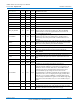
3.1 Normal Operating Conditions
Normal Operating Conditions
Operating Voltage 1.8-V Core, (135 MHz), 3.3-V I/O
Operating Ambient Temperature Range
-40C to 85C
Storage Temperature Range
-65C to 150C
Junction Temperature Range
-40C to 150C
Table 3 Normal Operating Conditions
Long-term high-temperature storage and/or extended use at maximum temperature conditions may result in a reduction of
overall device life. For additional information, see IC Package Thermal Metrics Application Report (TI literature number
SPRA953) and Reliability Data for additional information; see IC Package Thermal Metrics Application Report and Reliability
Data (TI literature number SPRA953).
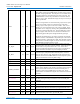
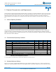
3.2 Recommended Operating Conditions
Parameter Min Nom Max Unit
3v3 Device Supply Voltage, I/O 3.14 3.3 3.47 V
1v8 Device Supply Voltage, CPU 1.8 V (135MHz) 1.71 1.8 1.89 V
V
IH
High-level input voltage All inputs except X1/XCLKIN 2.0 - 3v3 V
V
IL
Low-level input voltage All inputs except X1/XCLKIN 0.8 V
V
IH
High-level input voltage X1/XCLKIN (@50uA max) .7(1v8) - 1v8 V
V
IL
Low-level input voltage X1/XCLKIN (@50uA max) 0.3(1v8) V
f
SYSCLKOUT
Device clock frequency (system clock) = 1.8 V ± 5% 29.4912 MHz
I
OH
High-level output current source current, V
OH
= 2.4 V -4 mA
I
OH
High-level output current source current, V
OH
= 2.4 V (See
Note) ††
-8 mA
I
OL
Low-level output sink current V
OL
= V
OL
MAX 4 mA
I
OL
Low-level output sink current V
OL
= V
OL
MAX (Group 2) 8 mA
Table 4 Recommended Operating Conditions
†† Note Applies to the following pin: SPI_WAKE (TQFP Pin 106, BGA Pin D9).
3.3 Absolute Maximum Ratings
Stresses in excess of the Absolute Maximum Ratings can cause permanent damage to the device. These are absolute stress
ratings only. Functional operation of the device is not implied at these or any other conditions in excess of those given in the