
Datasheet

BST39
Document number: DS33021 Rev. 5 - 2
2 of 7
www.diodes.com
July 2014
© Diodes Incorporated
BST39
A
Product Line o
f
Diodes Incorporated
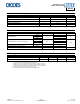
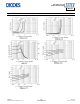
Absolute Maximum Ratings (@T
A
= +25°C, unless otherwise specified.)
Characteristic Symbol Value Unit
Collector-Base Voltage
V
CBO
400 V
Collector-Emitter Voltage
V
CEO
350 V
Emitter-Base Voltage
V
EBO
7 V
Continuous Collector Current
I
C
500 mA
Peak Pulse Current
I
CM
1 A
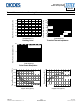
Thermal Characteristics (@T
A
= +25°C, unless otherwise specified.)
Characteristic Symbol Value Unit
Power Dissipation
(Note 5)
P
D
1
W
(Note 6) 1.5
(Note 7) 2.0
Thermal Resistance, Junction to Ambient Air
(Note 5)
R
θJA
125
°C/W
(Note 6) 83
(Note 7) 60
Thermal Resistance, Junction to Lead (Note 8)
R
θJL
22
Thermal Resistance, Junction to Case (Note 9)
R
θJC
16
Operating and Storage Temperature Range
T
J,
T
STG
-55 to +150 °C
ESD Ratings (Note 10)
Characteristic Symbol Value Unit JEDEC Class
Electrostatic Discharge - Human Body Model ESD HBM 4,000 V 3A
Electrostatic Discharge - Machine Model ESD MM 400 V C
Notes: 5. For a device mounted with the exposed collector pad on 15mm x 15mm 1oz copper that is on a single-sided 1.6mm FR4 PCB; device is measured
under still air conditions whilst operating in a steady-state.
6. Same as Note 5, except the device is mounted on 25mm x 25mm 1oz copper.
7. Same as Note 5, except the device is mounted on 50mm x 50mm 1oz copper.
8. Thermal resistance from junction to solder-point (on the exposed collector pad).
9. Thermal resistance from junction to the top of the case.
10. Refer to JEDEC specification JESD22-A114 and JESD22-A115.