
Datasheet
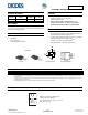


DMG9N65CTI
Document number: DS36027 Rev. 4 - 2
2 of 5
www.diodes.com
February 2015
© Diodes Incorporated
DMG9N65CTI
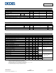
Maximum Ratings (@T
A
= +25°C, unless otherwise specified.)
Characteristic
Symbol
Value
Unit
Drain-Source Voltage
V
DSS
650
V
Gate-Source Voltage
V
GSS
±30
V
Continuous Drain Current (Notes 5 & 6)
V
GS
= 10V
Steady
State
T
C
= +25°C
T
C
= +70°C
I
D
9.0
7.0
A
Pulsed Drain Current (Note 7) 10µs pulse, pulse duty cycle<=1%
I
DM
30
A
Avalanche Current (Note 8) V
DD
= 100V, V
GS
= 10V, L = 60mH
I
AR
2.7
A
Repetitive avalanche energy (Note 8) V
DD
= 100V, V
GS
= 10V, L = 60mH
E
AR
260
mJ
Thermal Characteristics
Characteristic
Symbol
Max
Unit
Power Dissipation (Note 5)
T
C
= +25°C
T
C
= +70°C
P
D
13
8
W
Thermal Resistance, Junction to Case (Note 5)
T
C
= +25°C
R
θJC
8.84
°C/W
Operating and Storage Temperature Range
T
J
, T
STG
-55 to +150
°C
Electrical Characteristics (@T
A
= +25°C, unless otherwise specified.)
Characteristic
Symbol
Min
Typ
Max
Unit
Test Condition
OFF CHARACTERISTICS (Note 9)
Drain-Source Breakdown Voltage
BV
DSS
650
-
-
V
V
GS
= 0V, I
D
= 250µA
Zero Gate Voltage Drain Current T
J
= +25°C
I
DSS
-
-
1.0
µA
V
DS
= 650V, V
GS
= 0V
Gate-Source Leakage
I
GSS
-
-
±100
nA
V
GS
= ±30V, V
DS
= 0V
ON CHARACTERISTICS (Note 9)
Gate Threshold Voltage
V
GS(th)
3
-
5
V
V
DS
= V
GS
, I
D
= 250μA
Static Drain-Source On-Resistance
R
DS (ON)
-
0.7
1.3
Ω
V
GS
= 10V, I
D
= 4.5A
Forward Transfer Admittance
|Y
fs
|
-
8.5
-
S
V
DS
= 40V, I
D
= 4.5A
Diode Forward Voltage
V
SD
-
0.7
1.0
V
V
GS
= 0V, I
S
= 1A
DYNAMIC CHARACTERISTICS (Note 10)
Input Capacitance
C
iss
-
2310
-
pF
V
DS
= 25V, V
GS
= 0V,
f = 1.0MHz
Output Capacitance
C
oss
-
122
-
Reverse Transfer Capacitance
C
rss
-
2.2
-
Gate Resistance
R
g
-
2.2
-
Ω
V
DS
= 0V, V
GS
= 0V, f = 1MHz
Total Gate Charge V
GS
= 10V
Q
g
-
39
-
nC
V
GS
= 10V, V
DS
= 520V,
I
D
= 8A
Gate-Source Charge
Q
gs
-
8.5
-
Gate-Drain Charge
Q
gd
-
11.9
-
Turn-On Delay Time
t
D(on)
-
39
-
ns
V
GS
= 10V, V
DS
= 325V,
R
G
= 25Ω, I
D
= 8A
Turn-On Rise Time
t
r
-
29
-
ns
Turn-Off Delay Time
t
D(off)
-
122
-
ns
Turn-Off Fall Time
t
f
-
28
-
ns
Body Diode Reverse Recovery Time
t
rr
-
570
-
ns
dI/dt = 100A/µs, V
DS
= 100V,
I
F
= 8A
Body Diode Reverse Recovery Charge
Q
rr
-
4.17
-
µC
Notes: 5. Device mounted on an infinite heatsink.
6. Drain current limited by maximum junction temperature.
7. Repetitive rating, pulse width limited by junction temperature.
8. I
AR
and E
AR
rating are based on low frequency and duty cycles to keep T
J
= +25°C.
9. Short duration pulse test used to minimize self-heating effect.
10. Guaranteed by design. Not subject to production testing.