
Datasheet


ZLDO1117
Document number: DS32018 Rev. 6 - 2
3 of 14
www.diodes.com
July 2012
© Diodes Incorporated
ZLDO1117
A
Product Line o
f
Diodes Incorporated
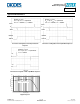
Recommended Operating Conditions (@T
A
= +25°C, unless otherwise specified.)
Symbol Parameter Min Max Unit
V
IN
Input voltage 2.7 (Note 8) 18 V
I
O
Output current 0.01 1 A
T
J
Operating Junction Temperature Range (Note 5) -40 +125 °C
Package Thermal Data
Thermal Resistance Package Rating Unit
Junction-to-Ambient, θ
JA
SOT223 (Note 6)
TO252 (Note 7)
107
73
°C/W
Junction-to-Case, θ
JC
SOT223 (Note 6)
TO252 (Note 7)
16
12
°C/W
Notes: 5. ZLDO1117 contains an internal thermal limiting circuit that is designed to protect the regulator in the event that the maximum junction temperature
exceeded. When activated, typically at 150°C, the regulator Output switches off and then back on as the die cools.
6. Test condition for SOT223: T
A
= +27°C, no air flow, device mounted on 2”X2” polyimide PCB, 2 oz copper, 5.6mmX5.6mm pad.
7. Test condition for TO252: T
A
= +27°C, no air flow, device mounted on 2”X2” polyimide PCB, 1 oz copper, 2cmX2cm pad.
8. Ensures correct operation without entering dropout. Device will continue to operate below this minimum input voltage under dropout conditions.
Electrical Characteristics (@T
A
= +25°C, unless otherwise specified.)
Parameter Conditions T
A
Min Typ Max Unit
Reference Voltage ZLDO1117-ADJ
(V
IN
-V
OUT
) = 2V, I
O
= 10mA 25 1.238 1.250 1.263
V
V
OUT
+1.4V < V
IN
< 10V,
10mA < I
O
< 1A
FT 1.225 1.275
Output Voltage
ZLDO1117-1.2
I
O
= 10mA, V
IN
= 3.2V 25 1.188 1.200 1.212 V
10mA< I
O
< 1A, 2.7V <V
IN
< 12V FT 1.176 1.224
ZLDO1117-1.5
I
O
= 10mA, V
IN
= 3.5V 25 1.485 1.500 1.515
V
0 < I
O
< 1A, 2.9V <V
IN
< 12V FT 1.470 1.530
ZLDO1117-1.8
I
O
= 10mA, V
IN
= 3.8V 25 1.782 1.800 1.818
V
0 < I
O
< 1A, 3.2V <V
IN
< 12V FT 1.764 1.836
ZLDO1117-2.5
I
O
= 10mA, V
IN
= 4.5V 25 2.475 2.500 2.525
V
0 < I
O
< 1A, 3.9V <V
IN
< 12V FT 2.450 2.550
ZLDO1117-3.3
I
O
= 10mA, V
IN
= 5.3V 25 3.267 3.300 3.333
V
0 < I
O
< 1A, 4.7V <V
IN
< 12V FT 3.235 3.365
ZLDO1117-5.0
I
O
= 10mA, V
IN
= 7V 25 4.95 5.000 5.05
V
0 < I
O
< 1A, 6.4V <V
IN
< 12V FT 4.900 5.100
Line Regulation
ZLDO1117-ADJ
ZLDO1117-1.2
I
O
= 10mA,
V
OUT
+1.5V<V
IN
<12V
25 0.1
%
FT 0.2
ZLDO1117-xx
I
O
= 0mA,
V
OUT
+1.5V<V
IN
<12V
25 0.1
%
FT 0.2
Notes: 9. See thermal regulation specifications for changes in output voltage due to heating effects. Line and load regulation are measured at a constant
junction temperature by low duty cycle pulse testing. Load regulation is measured at the output lead = 1/18” from the package.
10. Line and load regulation are guaranteed up to the maximum power dissipation of 15W. Power dissipation is determined by the difference between input
and output differential and the output current. Guaranteed maximum power dissipation will not be available over the full input/output range.