
Datasheet


ZLDO1117
Document number: DS32018 Rev. 6 - 2
4 of 14
www.diodes.com
July 2012
© Diodes Incorporated
ZLDO1117
A
Product Line o
f
Diodes Incorporated
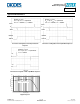
Electrical Characteristics (cont.) (@T
A
= +25°C, unless otherwise specified.)
Parameter Conditions T
A
Min Typ Max Unit
Load Regulation
ZLDO1117-ADJ
V
IN
=3.3V,V
ADJ
=0, 10mA<I
O
<1A,
(Notes 9, 10)
25 0.2
%
FT
0.4
ZLDO1117-1.2
V
IN
=2.7V, 10mA < I
O
< 1A,
(Notes 9, 10)
25 0.2 %
FT 0.4
ZLDO1117-1.5
V
IN
= 3V, 0 < I
O
< 1A,
(Notes 9, 10)
25 3
mV
FT 6
ZLDO1117-1.8
V
IN
= 3.3V, 0 < I
O
< 1A,
(Notes 9, 10)
25 4
mV
FT 8
ZLDO1117-2.5
V
IN
= 4V, 0 < I
O
< 1A,
(Notes 9, 10)
25 5
mV
FT 10
ZLDO1117-3.3
V
IN
= 4.8V, 0 < I
O
< 1A,
(Notes 9, 10)
25 6.6
mV
FT 13
ZLDO1117-5.0
V
IN
= 6.5V, 0 < I
O
< 1A,
(Notes 9, 10)
25 10
mV
FT 20
Dropout Voltage
(V
IN
-V
OUT
)
ZLDO1117-
ADJ/1.2/1.5/1.8/2.5/
3.3/5.0
I
O
= 1A, ΔV
OUT
= 1%V
OUT
25 1.11 1.2
V
0 ~ 125
1.3
FT
1.35
Current Limit
ZLDO1117-
ADJ/1.2/1.5/1.8/2.5/
3.3/5.0
(V
IN
-V
OUT
) = 5V
25
A
FT 1. 1
Minimum Load Current
(Note 8)
ZLDO1117-ADJ
ZLDO1117-1.2
V
IN
= <18V FT 2 5 mA
Quiescent current
ZLDO1117-xx V
IN
< 18V, I
O
= 0mA
FT 4 10 mA
GND current
ZLDO1117-ADJ
ZLDO1117-1.2
V
IN
= 7V FT 35 120 µA
Thermal Regulation
30ms pulse
25 0.1 %/W
Ripple Rejection
f = 120Hz, C
OUT
= 25µF Tantalum,
I
OUT
= 100mA, ZLDO1117-XXX V
IN
= V
OUT
+3V
25 60 80 dB
Temperature Stability
I
O
= 10mA
0.5 %
Notes: 8. See thermal regulation specifications for changes in output voltage due to heating effects. Line and load regulation are measured at a constant
junctiontemperature by low duty cycle pulse testing. Load regulation is measured at the output lead = 1/18” from the package.
9. Line and load regulation are guaranteed up to the maximum power dissipation of 15W. Power dissipation is determined by the difference between input
and output differential and the output current. Guaranteed maximum power dissipation will not be available over the full input/output range.