
Manual

2DD1621T
NPN SURFACE MOUNT TRANSISTOR
Features
NEW PRODUCT
• Epitaxial Planar Die Construction
• Ideally Suited for Automated Assembly Processes
• Ideal for Medium Power Switching or Amplification Applications
• Lead Free By Design/RoHS Compliant (Note 1)
• "Green" Device (Note 2)
Mechanical Data
• Case: SOT89-3L
• Case Material: Molded Plastic, "Green” Molding Compound.
UL Flammability Classification Rating 94V-0
• Moisture Sensitivity: Level 1 per J-STD-020D
• Terminals: Finish — Matte Tin annealed over Copper leadframe
(Lead Free Plating). Solderable per MIL-STD-202, Method 208
• Marking Information: See Page 3
• Ordering Information: See Page 3
• Weight: 0.072 grams (approximate)
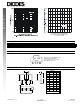
SOT89-3L
3
1
2,4
C
O
L
L
E
C
T
O
R
E
M
I
T
T
E
R
B
A
S
E
4
3
2
1
C
C
B
E
T
O
P
V
I
E
W
Schematic and Pin Configuration
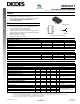
Maximum Ratings @T
A
= 25°C unless otherwise specified
Characteristic Symbol Value Unit
Collector-Base Voltage
V
CBO
30 V
Collector-Emitter Voltage
V
CEO
25 V
Emitter-Base Voltage
V
EBO
6.0 V
Collector Current
I
C
2.0 A
Thermal Characteristics
Characteristic Symbol Value Unit
Power Dissipation (Note 3) @ T
A
= 25°C P
D
1 W
Thermal Resistance, Junction to Ambient Air (Note 3) @T
A
= 25°C
R
θ
JA
125 °C/W
Operating and Storage Temperature Range
T
J
, T
STG
-55 to +150 °C
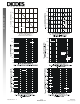
Electrical Characteristics @T
A
= 25°C unless otherwise specified
Characteristic Symbol Min Typ Max Unit Test Conditions
OFF CHARACTERISTICS (Note 4)
Collector-Base Breakdown Voltage
V
(BR)CBO
30
⎯ ⎯
V
I
C
= 10μA, I
E
= 0
Collector-Emitter Breakdown Voltage
V
(BR)CEO
25
⎯ ⎯
V
I
C
= 1mA, I
B
= 0
Emitter-Base Breakdown Voltage
V
(BR)EBO
6.0
⎯ ⎯
V
I
C
= 10μA, I
C
= 0
Collector-Base Cutoff Current
I
CBO
⎯ ⎯
100 nA
V
CB
= 20V, I
E
= 0
Emitter-Base Cutoff Current
I
EBO
⎯ ⎯
100 nA
V
EB
= 4.0V, I
C
= 0
ON CHARACTERISTICS (Note 4)
DC Current Gain
h
FE
200
65
⎯
⎯
400
⎯
⎯
V
CE
= 2.0V, I
C
= 0.1A
V
CE
= 2.0V, I
C
= 1.5A
Collector-Emitter Saturation Voltage
V
CE(SAT)
⎯
0.12 0.4 V
I
C
= 1.5A, I
B
= 75mA
Base-Emitter Saturation Voltage
V
BE(SAT)
⎯
0.9 1.2 V
I
C
= 1.5A, I
B
= 75mA
SMALL SIGNAL CHARACTERISTICS
Current Gain-Bandwidth Product
f
T
⎯
300
⎯
MHz
V
CE
= 10V, I
C
= 50mA,
f = 100MHz
Output Capacitance
C
obo
⎯
16
⎯
pF
V
CB
= 10V, I
E
= 0, f = 1MHz
SWITCHING CHARACTERISTICS
Turn On Time
t
on
⎯
70
⎯
ns
Storage Time
t
stg
⎯
170
⎯
ns
Fall Time
t
f
⎯
25
⎯
ns
V
CE
= 12V, V
BE
= 5V,
I
B1
= I
B2
= 25mA, I
C
= 500mA
Notes: 1. No purposefully added lead.
2. Diodes Inc.'s "Green" policy can be found on our website at http://www.diodes.com/products/lead_free/index.php.
3. Device mounted on FR-4 PCB; pad layout as shown on page 4 or in Diodes Inc. suggested pad layout document AP02001, which can
be found on our website at http://www.diodes.com/datasheets/ap02001.pdf.
4. Measured under pulsed conditions. Pulse width = 300μs. Duty cycle ≤2%.
DS31240 Rev. 2 - 2
1 of 4
www.diodes.com
2DD1621T
© Diodes Incorporated
Please click here to visit our online spice models database.