
Instruction Manual

74LVC1G04
Document number: DS32198 Rev. 7 - 2
6 of 15
www.diodes.com
March 2014
© Diodes Incorporated
NEW PRODUCT
74LVC1G04
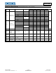
Package Characteristics (All typical values are at V
CC
= 3.3V, T
A
= +25°C)
Symbol Parameter Test Conditions V
CC
Min Typ. Max Unit
θ
JA
Thermal Resistance
Junction-to-Ambient
SOT25
(Note 9)
— 204 —
°C/W
SOT353 — 371 —
SOT553 — 231 —
X2-DFN0808-4 — 400 —
X1-DFN1010-6 — 435 —
X2-DFN1010-6 — 445 —
X2-DFN1409-6 — 470 —
X2-DFN1410-6 — 460 —
θ
JC
Thermal Resistance
Junction-to-Case
SOT25
(Note 9)
— 52 —
°C/W
SOT353 — 143 —
SOT553 — 105 —
X2-DFN0808-4 — 225 —
X1-DFN1010-6 — 250 —
X2-DFN1010-6 — 250 —
X2-DFN1409-6 — 275 —
X2-DFN1410-6 — 265 —
Note: 9. Test condition for each of the 8 package types: Device mounted on FR-4 substrate PC board, 2oz copper, with minimum recommended pad layout.
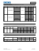
Switching Characteristics
Figure 1 Typical Values at T
A
= +25°C and nominal voltages 1.8V, 2.5V, 2.7V, 3.3V, and 5.0V.
Parameter
From
Input
To
Output
V
CC
T
A
= -40°C to +85°C T
A
= -40°C to +125°C
Unit
Min Typ Max Min Max
t
pd
A or B Y
1.8V ± 0.15V 1.0 3.0 7.5 1.0 9.5
ns
2.5V ± 0.2V 0.5 2.0 5.0 0.5 6.5
2.7V 0.5 2.3 5.2 0.5 7.0
3.3V ± 0.3V 0.5 2.0 4.2 0.5 5.5
5.0V ± 0.5V 0.5 1.6 3.7 0.5 5.0
Operating Characteristics
T
A
= +25°C
Parameter
Test
Conditions
V
CC
= 1.8V V
CC
= 2.5V V
CC
= 3.3V V
CC
= 5V
Unit
Typ. Typ. Typ. Typ.
C
pd
Power Dissipation
Capacitance
f = 10MHz 16 16 16 16 pF