
Instruction Manual

DUAL OP AMP AND VOLTAGE REFERENCE AP4310/A
5
Jan. 2013 Rev. 1. 8 BCD Semiconductor Manufacturing Limited
Data Sheet
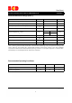
Operating Conditions: V
CC
=+5V, T
A
=25
o
C unless otherwise specified.
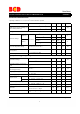
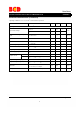
Electrical Characteristics
Parameter Conditions Min Typ Max Unit
Total Supply Current, excluding Cur-
rent in Voltage Reference
V
CC
=5V, no load, -40
o
C≤T
A
≤105
o
C
0.15 0.25
mA
V
CC
=30V, no load, -40
o
C≤T
A
≤105
o
C
0.20 0.30
Voltage Reference Section
Reference Voltage
AP4310A
I
K
=10mA
T
A
=25
o
C
2.49 2.50 2.51
V
-40
o
C≤T
A
≤105
o
C
2.48 2.50 2.52
AP4310
T
A
=25
o
C
2.475 2.50 2.525
V
-40
o
C≤T
A
≤105
o
C
2.45 2.50 2.55
Reference Voltage Deviation
Over Full Temperature Range
I
K
=10mA, T
A
=-40 to 105
o
C
524mV
Minimum Cathode Current
for Regulation
0.01 0.05 mA
Dynamic Impedance
I
K
=1.0 to 80mA, f<1kHz
0.2 0.5 Ω
Op Amp 1 Section (V
CC
=5V, V
O
=1.4V, T
A
=25
o
C, unless otherwise noted)
Input Offset Voltage
T
A
=25
o
C
0.5
3
mV
T
A
=-40 to 105
o
C
5
Input Offset Voltage Temperature
Drift
T
A
=-40 to 105
o
C
7
µV/
o
C
Input Bias Current
(Inverting Input Only)
T
A
=25
o
C
20
150 nA
Large Signal Voltage Gain
V
CC
=15V, R
L
=2kΩ, V
O
=1.4 to 11.4V
85
100
dB
Power Supply Rejection Ratio
V
CC
=5 to 30V
70
90
dB
Output Current
Source
V
CC
=15V, V
ID
=1V, V
O
=2V
20
40
mA
Sink
V
CC
=15V, V
ID
=-1V, V
O
=2V
520
mA
Output Voltage Swing (High)
V
CC
=30V, R
L
=10kΩ, V
ID
=1V
27
28
V
Output Voltage Swing (Low)
V
CC
=30V, R
L
=10kΩ, V
ID
=-1V
17
100 mV
Slew Rate
V
CC
=18V, R
L
=2kΩ, A
V
=1,
V
IN
=0.5 to 2V, C
L
=100pF
0.2 0.5 V/µ s
Unity Gain Bandwidth
V
CC
=30V, R
L
=2kΩ, C
L
=100pF
0.7 1.0 MHz