
User guide
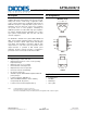
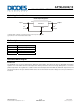


AP78L05/08/12
AP78LXX SERIES 3-TERMINAL POSITIVE REGULATORS
AP78L05/08/12
Document number: DS31054 Rev. 10 - 2
4 of 16
www.diodes.com
March 2012
© Diodes Incorporated
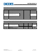
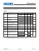
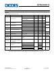
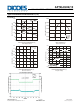
AP78Lxx Electrical Characteristics (All Output Voltage Versions)
Limits in standard typeface are for T
A
= 25℃, Bold typeface applies over T
J
= -20°C to +125°C for TO92, SOT89 and SO-8 packages.
Unless otherwise specified: I
O
= 40mA, C
I
= 0.33µF, C
O
= 0.1µF.
AP78L05
Unless otherwise specified, V
IN
= 10V
Symbol Parameter Conditions Min Typ. Max Unit
V
O
Output Voltage
4.8 5 5.2
V
7V ≤ V
IN
≤ 20V
1mA ≤ I
O
≤ 40mA
4.75
5.25
1mA ≤ I
O
≤ 70mA 4.75
5.25
ΔV
O
Line Regulation
7V ≤ V
IN
≤ 20V
18 75
mV
8V ≤ V
IN
≤ 20V
10 54
ΔV
O
Load Regulation
1mA ≤ I
O
≤ 100mA
20 60
mV
1mA ≤ I
O
≤ 40mA
5 30
I
Q
Quiescent Current 3 5
mA
ΔI
Q
Quiescent Current Change
8V ≤ V
IN
≤ 20V
1.0
1mA ≤ I
O
≤ 40mA
0.1
V
N
Output Noise Voltage
f = 10Hz to 100kHz
(Note 4)
- 40 µV
ΔV
IN
/ΔV
OUT
Ripple Rejection
f = 120Hz
8V ≤ V
IN
≤ 16V
47 62 dB
I
PK
Peak Output Current 140 mA
ΔV
O
/ΔT
Average Output Voltage Tempco
I
O
= 5mA
-0.65 mV/
o
C
V
IN(MIN)
Minimum Value of Input Voltage
Required to Maintain Line Regulation
6.7 7 V
θ
JA
Thermal Resistance Junction to
Ambient
TO92 (Note 5)
176
o
C/W
SO-8 (Note 6) 153
SOT89 (Note 7) 145
θ
JC
Thermal Resistance Junction to Case
TO92 (Note 5)
33
SO-8 (Note 6) 18
SOT89 (Note 7) 25
Notes: 4. Recommend 0.01µF minimum load capacitance at output to suppress high frequency noise.
5. Test conditions for TO92: No heat sink, no air flow.
6. Test conditions for SO-8: Device mounted on 2oz copper, minimum recommended pad layout, FR-4 PCB.
7. Test conditions for SOT89: Device mounted on FR-4 substrate PC board, 2oz copper, with minimum recommended pad layout.