
Instruction Manual

D1213A-01LP4
Document number: DS35760 Rev. 5 - 2
2 of 4
www.diodes.com
August 2012
© Diodes Incorporated
D1213
A
-01LP4
NEW PRODUCT
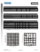
Maximum Ratings (@T
A
= +25°C, unless otherwise specified.)
Characteristic Symbol Value Unit Conditions
Peak Pulse Current
I
PP
5 A
8/20μs, Per Figure 2
ESD Protection – Contact Discharge
V
ESD
_
Contac
t
±8 kV
Standard IEC 61000-4-2
ESD Protection – Air Discharge
V
ESD
_
Ai
r
±15 kV
Standard IEC 61000-4-2
Thermal Characteristics
Characteristic Symbol Value Unit
Package Power Dissipation (Note 5)
P
D
250 mW
Thermal Resistance, Junction to Ambient (Note 5)
R
θ
JA
500
°C/W
Operating and Storage Temperature Range T
J
, T
STG
-65 to +150
°C
Electrical Characteristics (@T
A
= +25°C, unless otherwise specified.)
Characteristic Symbol Min Typ Max Unit Test Conditions
Reverse working voltage VRWM — — 3.3 V —
Reverse current (Note 6)
I
R
— 0.1 1.0 μA
V
R
= V
RWM
= 3.3V
Reverse breakdown voltage VBR 6.0 — — V
I
R
= 1mA
Forward voltage
V
F
0.6 0.8 0.95 V
I
F
= 8mA
Reverse clamping voltage, Positive Transients
V
CL1
— 10.0 — V
I
PP
= 1A, t
p
= 8/20μs
Reverse clamping voltage, Negative Transients
V
CL2
— -1.7 — V
I
PP
= -1A, t
p
= 8/20μs
Dynamic resistance
R
DYN
— 0.9 — Ω
I
R
= 1A, t
p
= 8/20μs
Capacitance
C
T
— 0.85 1.2 pF
V
R
= 1.65V, f = 1MHz
Notes: 5. Device mounted on FR-4 PCB pad layout (2oz copper) as shown on Diodes, Inc. suggested pad layout AP02001, which can be found on our website at
http://www.diodes.com.
6. Short duration pulse test used to minimize self-heating effect.
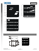
0 25 50 75 100 125 150 175 200
100
75
50
25
0
T , AMBIENT TEMPERATURE (°C)
Fig. 1 Pulse Derating Curve
A
P
EAK
P
U
LSE DE
R
A
T
IN
G
IN %
O
F
PEAK POWER OR CURRENT
0
t, TIME ( s)
Fig. 2 Pulse Waveform
μ
20 40
60
100
50
0
I , PEAK PULSE CURRENT (%I )
PppP