
User guide

DESD5V0S1BLP3
Document number: DS36257 Rev. 1 - 2
2 of 4
www.diodes.com
September 2013
© Diodes Incorporated
DESD5V0S1BLP3
NEW PRODUCT
NEW PRODUCT
Maximum Ratings (@T
A
= +25°C, unless otherwise specified.)
Characteristic Symbol Value Unit Conditions
Peak Pulse Power Dissipation
P
PP
145 W 8/20µs, Per Figure 3
Peak Pulse Current
I
PP
10 A 8/20µs, Per Figure 3
ESD Protection – Contact Discharge
V
ESD_Contact
±30 kV Standard IEC 61000-4-2
ESD Protection – Air Discharge
V
ESD_Air
±30 kV Standard IEC 61000-4-2
Thermal Characteristics
Characteristic Symbol Value Unit
Package Power Dissipation (Note 5)
P
D
250 mW
Thermal Resistance, Junction to Ambient (Note 5)
R
JA
500 °C/W
Operating and Storage Temperature Range
T
J
, T
STG
-65 to +150 °C
Electrical Characteristics (@T
A
= +25°C, unless otherwise specified.)
Characteristic Symbol Min Typ Max Unit Test Conditions
Reverse Standoff Voltage
V
RWM
— — 5 V —
Channel Leakage Current (Note 6)
I
RM
— 1 100 nA
V
RWM
= 5V
Clamping Voltage, Positive Transients
V
CL
— — 10 V
I
PP
= 1A, tp = 8/20μS
— — 14.5 V
I
PP
= 10A, tp = 8/20μS
Breakdown Voltage
V
BR
6 — 9.5 V
I
R
= 1mA
Differential Resistance
R
DIF
— 0.5 — Ω
I
PP
= 10A, t
p
= 8/20µs
Channel Input Capacitance
C
T
— 22 28
pF
V
R
= 0V, f = 1MHz
— 16 22
V
R
= 5V, f = 1MHz
Notes: 5. Device mounted on FR-4 PCB pad layout (2oz copper) as shown on Diodes, Inc. suggested pad layout AP02001, which can be found on our website at
http://www.diodes.com.
6. Short duration pulse test used to minimize self-heating effect.
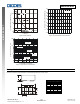
0125175
150
50
100
0
T , AMBIENT TEMPERATURE ( C)
Figure 1 Power Derating Curve
A
°
P
,
P
O
WE
R
DISSI
P
A
T
I
O
N (mW)
D
25 10050 75 150
25
75
125
250
175
Note 5
200
225
0
50
25 50
75 100 125
150
P
EAK
P
U
LSE DE
R
A
T
I
N
G
%
O
F
PEAK POWER OR CURRENT
T , AMBIENT TEMPERATURE (°C)
Figure 2 Pulse Derating Curve
A
0
100
25
75
175 200