
Manual

DF005S – DF10S
Document number: DS17001 Rev. 16 - 2
2 of 5
www.diodes.com
August 2013
© Diodes Incorporated
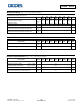
DF005S
–
DF10S
Maximum Ratings (@T
A
= +25°C, unless otherwise specified.)
Single phase, half wave, 60Hz, resistive or inductive load
For capacitive load, derate current by 20%.
Characteristic Symbol
DF
005S
DF
01S
DF
02S
DF
04S
DF
06S
DF
08S
DF
10S
Unit
Peak Repetitive Reverse Voltage
Working Peak Reverse Voltage
DC Blocking Voltage
V
RMM
V
RWM
V
R
50 100 200 400 600 800 1000 V
RMS Reverse Voltage
V
RMS
35 70 140 280 420 560 700 V
Average Forward Rectified Current @ T
A
= +40°C I
O
1.0 A
Non-Repetitive Peak Forward Surge Current, 8.3 ms
Single Half Sine-Wave Superimposed on Rated Load
I
FSM
50 A
Non-Repetitive Peak Forward Surge Current, 1.0 ms
Single Half Sine-Wave Superimposed on Rated Load
I
FSM
100 A
Thermal Characteristics
Characteristic Symbol
DF
005S
DF
01S
DF
02S
DF
04S
DF
06S
DF
08S
DF
10S
Unit
Typical Thermal Resistance, Junction to Ambient (Note 2)
R
θJA
+40 °C/W
Operating and Storage Temperature Range
T
J
, T
STG
-65 to +150 °C
Electrical Characteristics (@T
A
= +25°C, unless otherwise specified.)
Characteristic Symbol
DF
005S
DF
01S
DF
02S
DF
04S
DF
06S
DF
08S
DF
10S
Unit
Forward Voltage (per element) @ I
F
= 1.0A V
FM
1.1 V
Peak Reverse Current at Rated @ T
A
= +25°C
DC Blocking Voltage (per element) @ T
A
= +125°C
I
RM
10
500
µA
I
2
t Rating for Fusing (t<8.3ms) I
2
t 10.4 A
2
s
Typical Total Capacitance (per element) (Note 1)
C
T
25 pF