
User Manual


DMC3032LSD
Document number: DS32153 Rev. 1 - 2
1 of 8
www.diodes.com
May 2010
© Diodes Incorporated
DMC3032LSD
NEW PRODUCT
COMPLEMENTARY PAIR ENHANCEMENT MODE MOSFET
Features
• Low On-Resistance
• N-Channel: 32mΩ @ 10V
46mΩ @ 4.5V
• P-Channel: 39mΩ @ 10V
53mΩ @ 4.5V
• Low Input Capacitance
• Fast Switching Speed
• Low Input/Output Leakage
• Complementary Pair MOSFET
• Lead Free/RoHS Compliant (Note 1)
• "Green" Device (Note 2)
• Qualified to AEC-Q101 Standards for High Reliability
Mechanical Data
• Case: SO-8
• Case Material: Molded Plastic, “Green” Molding Compound.
UL Flammability Classification Rating 94V-0
• Moisture Sensitivity: Level 1 per J-STD-020
• Terminals Connections: See Diagram
• Terminals: Finish - Matte Tin annealed over Copper lead frame.
Solderable per MIL-STD-202, Method 208
• Marking Information: See Page 6
• Ordering Information: See Page 6
• Weight: 0.072 grams (approximate)
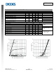
Maximum Ratings N-CHANNEL – Q1 @T
A
= 25°C unless otherwise specified
Characteristic Symbol Value Unit
Drain-Source Voltage
V
DSS
30 V
Gate-Source Voltage
V
GSS
±20 V
Continuous Drain Current (Note 3)
Steady
State
T
A
= 25°C
T
A
= 85°C
I
D
8.1
5.1
A
Pulsed Drain Current (Note 4)
I
DM
25 A
Maximum Ratings P-CHANNEL – Q2 @T
A
= 25°C unless otherwise specified
Characteristic Symbol Value Unit
Drain-Source Voltage
V
DSS
-30 V
Gate-Source Voltage
V
GSS
±20 V
Continuous Drain Current (Note 3)
Steady
State
T
A
= 25°C
T
A
= 85°C
I
D
-7.0
-4.5
A
Pulsed Drain Current (Note 4)
I
DM
-25 A
Thermal Characteristics @T
A
= 25°C unless otherwise specified
Characteristic Symbol Value Unit
Power Dissipation (Note 3)
P
D
2.5 W
Thermal Resistance, Junction to Ambient (Note 3)
R
θJA
50 °C/W
Operating and Storage Temperature Range
T
J
, T
STG
-55 to +150 °C
Notes: 1. No purposefully added lead.
2. Diodes Inc.'s "Green" policy can be found on our website at http://www.diodes.com/products/lead_free/index.php.
3. Device mounted on FR-4 PCB, with minimum recommended pad layout.
4. Repetitive rating, pulse width limited by junction temperature.
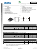
SO-8
Top View
Top View
D
1
S
1
G
1
D
2
S
2
G
2
N-Channel MOSFET P-Channel MOSFET
S2
D1
S1
D2
G1
G2
D2
D1