
Instruction Manual

DMC6040SSD
Document number: DS36829 Rev. 1 - 2
5 of 9
www.diodes.com
June 2014
© Diodes Incorporated
DMC6040SSD
ADVANCE INFORMATION
NEW PRODUCT
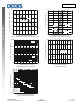
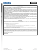
t1, PULSE DURATION TIME (sec)
Figure 12 Transient Thermal Resistance
r(t),
T
R
ANSIEN
T
T
H
E
R
MAL
R
ESIS
T
AN
C
E
R (t) = r(t) * R
R = 102°C/W
Duty Cycle, D = t1/ t2
θθ
θ
JA JA
JA
D = 0.5
D = 0.7
D = 0.9
D = 0.3
D = 0.1
D = 0.05
D = 0.02
D = 0.01
D = 0.005
D = Single Pulse
0.001
0.01
0.1
1
0.00001 0.0001 0.001 0.01 0.1 1 10 100 1000
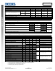
Electrical Characteristics P-Channel Q2 (@T
A
= +25°C, unless otherwise specified.)
Characteristic Symbol Min Typ Max Unit Test Condition
OFF CHARACTERISTICS (Note 8)
Drain-Source Breakdown Voltage
BV
DSS
-60
⎯ ⎯
V
V
GS
= 0V, I
D
= -250µA
Zero Gate Voltage Drain Current
I
DSS
⎯ ⎯
-1 µA
V
DS
= -48V, V
GS
= 0V
Gate-Source Leakage
I
GSS
⎯ ⎯
100 nA
V
GS
= ±16V, V
DS
= 0V
ON CHARACTERISTICS (Note 8)
Gate Threshold Voltage
V
GS
(
th
)
-1
⎯
-3 V
V
DS
= V
GS
, I
D
= -250µA
Static Drain-Source On-Resistance
R
DS (ON)
⎯
86 110
m
V
GS
= -10V, I
D
= -4.5A
⎯
98 130
V
GS
= -4.5V, I
D
=-3.5A
Diode Forward Voltage
V
SD
⎯
-0.7 -1.2 V
V
GS
= 0V, I
S
= -1A
DYNAMIC CHARACTERISTICS (Note 9)
Input Capacitance
C
iss
⎯
1030
⎯
pF
V
DS
= -30V, V
GS
= 0V, f = 1.0MHz
Output Capacitance
C
oss
⎯
49.1
⎯
Reverse Transfer Capacitance
C
rss
⎯
38.7
⎯
Gate Resistance
R
G
⎯
13.6
⎯
V
DS
= 0V, V
GS
= 0V, f = 1.0MHz
Total Gate Charge (V
GS
= -4.5V) Q
g
⎯
9.5
⎯
nC
V
DS
= -30V, I
D
= -5A
Total Gate Charge (V
GS
= -10V) Q
g
⎯
19.4
⎯
Gate-Source Charge
Q
g
s
⎯
2.3
⎯
Gate-Drain Charge
Q
g
d
⎯
3.6
⎯
Turn-On Delay Time
t
D
(
on
)
⎯
3.7
⎯
nS
V
GS
= -10V, V
DS
= -30V, R
GEN
= 6Ω,
I
D
= -5A
Turn-On Rise Time
t
r
⎯
6.3
⎯
Turn-Off Delay Time
t
D
(
off
)
⎯
58.7
⎯
Turn-Off Fall Time
t
f
⎯
26.1
⎯
Body Diode Reverse Recovery Time
t
r
r
⎯
14.85
⎯
nS
I
S
= -5A, dI/dt = 100A/s
Body Diode Reverse Recovery Charge
Q
r
r
⎯
8.8
⎯
nC
I
S
= -5A, dI/dt = 100A/s
Notes: 5. Device mounted on FR-4 substrate PC board, 2oz copper, with minimum recommended pad layout.
6. Device mounted on FR-4 substrate PC board, 2oz copper, with 1inch square copper plate.
7. UIS in production with L = 0.1mH, starting T
A
= +25°C.
8. Short duration pulse test used to minimize self-heating effect.
9. Guaranteed by design. Not subject to product testing.