
User guide
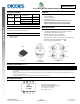

DMHC4035LSD
Document number: DS36287 Rev. 1 - 2
3 of 9
www.diodes.com
January 2014
© Diodes Incorporated
DMHC4035LSD
NEW PRODUCT
ADVANCE INFORMATION
NEW PRODUCT
Electrical Characteristics N-CHANNEL (@T
A
= +25°C, unless otherwise specified.)
Characteristic Symbol Min Typ Max Unit Test Condition
OFF CHARACTERISTICS (Note 6)
Drain-Source Breakdown Voltage
BV
DSS
40
— —
V
V
GS
= 0V, I
D
= 250A
Zero Gate Voltage Drain Current
I
DSS
— —
1 A
V
DS
= 40V, V
GS
= 0V
Gate-Source Leakage
I
GSS
— —
±100 nA
V
GS
= ±20V, V
DS
= 0V
ON CHARACTERISTICS (Note 6)
Gate Threshold Voltage
V
GS(th)
1 — 3 V
V
DS
= V
GS
, I
D
= 250A
Static Drain-Source On-Resistance
R
DS (ON)
—
26 45
m
V
GS
= 10V, I
D
= 3.9A
—
35 58
V
GS
= 4.5V, I
D
= 3.5A
Diode Forward Voltage
V
SD
—
0.7 1 V
V
GS
= 0V, I
S
= 1.25A
DYNAMIC CHARACTERISTICS (Note 7)
Input Capacitance
C
iss
— 574
—
pF
V
DS
= 20V, V
GS
= 0V,
f = 1MHz
Output Capacitance
C
oss
—
87.8
—
Reverse Transfer Capacitance
C
rss
—
38.7
—
Gate resistance
R
g
—
1.6
—
V
DS
= 0V, V
GS
= 0V, f = 1MHz
Total Gate Charge (V
GS
= 4.5V) Q
g
—
5.9
—
nC
V
DS
= 20V, I
D
= 3.9A
Total Gate Charge (V
GS
= 10V) Q
g
—
12.5
—
Gate-Source Charge
Q
gs
—
1.7
—
Gate-Drain Charge
Q
gd
—
2.2
—
Turn-On Delay Time
t
D(on)
—
3.1
—
ns
V
DD
= 20V, V
GS
= 10V,
R
L
= 20, R
G
= 6,
Turn-On Rise Time
t
r
—
2.6
—
Turn-Off Delay Time
t
D(off)
—
15
—
Turn-Off Fall Time
t
f
—
5.5
—
Reverse Recovery Time
t
rr
—
6.5
—
ns
I
F
= 3.9A, di/dt = 500A/s
Reverse Recovery Charge
Q
rr
—
1.2
—
nC
Electrical Characteristics P-CHANNEL (@T
A
= +25°C, unless otherwise specified.)
Characteristic Symbol Min Typ Max Unit Test Condition
OFF CHARACTERISTICS (Note 6)
Drain-Source Breakdown Voltage
BV
DSS
-40
—
— V
V
GS
= 0V, I
D
= -250A
Zero Gate Voltage Drain Current
I
DSS
— —
-1 A
V
DS
= -40V, V
GS
= 0V
Gate-Source Leakage
I
GSS
— —
±100 nA
V
GS
= ±20V, V
DS
= 0V
ON CHARACTERISTICS (Note 6)
Gate Threshold Voltage
V
GS(th)
-1 — -3 V
V
DS
= V
GS
, I
D
= -250A
Static Drain-Source On-Resistance
R
DS (ON)
—
49 65
m
V
GS
= -10V, I
D
= -4.2A
—
73 100
V
GS
= -4.5V, I
D
= -3.3A
Diode Forward Voltage
V
SD
—
-0.7 -1.2 V
V
GS
= 0V, I
S
= -1A
DYNAMIC CHARACTERISTICS (Note 7)
Input Capacitance
C
iss
—
587
—
pF
V
DS
= -20V, V
GS
= 0V,
f = 1MHz
Output Capacitance
C
oss
—
88.1
—
pF
Reverse Transfer Capacitance
C
rss
—
40.2
—
pF
Gate resistance
R
g
—
12.3
—
V
DS
= 0V, V
GS
= 0V, f = 1MHz
Total Gate Charge (V
GS
= -4.5V) Q
g
—
5.4
—
nC
V
DS
= -20V, I
D
= -4.2A
Total Gate Charge (V
GS
= -10V) Q
g
—
11.1
—
nC
Gate-Source Charge
Q
gs
—
1.5
—
nC
Gate-Drain Charge
Q
gd
—
2
—
nC
Turn-On Delay Time
t
D(on)
—
3.6
—
ns
V
DD
= -15V, V
GS
= -10V,
R
G
= 6, I
D
= -1A
Turn-On Rise Time
t
r
—
2.9
—
ns
Turn-Off Delay Time
t
D(off)
—
36.3
—
ns
Turn-Off Fall Time
t
f
—
15.3
—
ns
Reverse Recovery Time
t
rr
—
15.5
—
ns
I
F
= -4.2A, di/dt = 500A/s
Reverse Recovery Charge
Q
rr
—
16.9
—
nC
Notes: 6. Short duration pulse test used to minimize self-heating effect.
7. Guaranteed by design. Not subject to product testing.