
User Manual


DMN2041LSD
Document number: DS31964 Rev. 3 - 2
2 of 6
www.diodes.com
February 2014
© Diodes Incorporated
DMN2041LSD
NEW PRODUCT
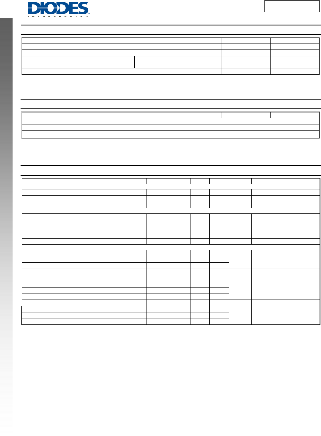
Maximum Ratings (@T
A
= +25°C, unless otherwise specified.)
Characteristic Symbol Value Units
Drain-Source Voltage
V
DSS
20 V
Gate-Source Voltage
V
GSS
12
V
Drain Current (Note 5) Steady
State
T
A
= +25°C
T
A
= +85°C
I
D
7.63
4.92
A
Pulsed Drain Current (Note 6)
I
DM
30 A
Thermal Characteristics
Characteristic Symbol Value Unit
Total Power Dissipation (Note 5)
P
D
1.16 W
Thermal Resistance, Junction to Ambient @T
A
= +25°C R
θJA
107.4 °C/W
Operating and Storage Temperature Range
T
J,
T
STG
-55 to +150 °C
Electrical Characteristics (@T
A
= +25°C, unless otherwise specified.)
Characteristic Symbol Min Typ Max Unit Test Condition
OFF CHARACTERISTICS (Note 7)
Drain-Source Breakdown Voltage
BV
DSS
20
—
— V
V
GS
= 0V, I
D
= 250μA
Zero Gate Voltage Drain Current T
J
= +25°C I
DSS
— —
1 μA
V
DS
= 20V, V
GS
= 0V
Gate-Source Leakage
I
GSS
— —
±100 nA
V
GS
= ±12V, V
DS
= 0V
ON CHARACTERISTICS (Note 7)
Gate Threshold Voltage
V
GS
(
th
)
0.5 — 1.2 V
V
DS
= V
GS
, I
D
= 250μA
Static Drain-Source On-Resistance
R
DS (ON)
—
19 28
mΩ
V
GS
= 4.5V, I
D
= 6A
25 41
V
GS
= 2.5V, I
D
= 5.2A
Forward Transfer Admittance
|Y
fs
|
— 6 — S
V
DS
= 10V, I
D
= 6A
Diode Forward Voltage
V
SD
— 0.7 1.2 V
V
GS
= 0V, I
S
= 1.7A
DYNAMIC CHARACTERISTICS (Note 8)
Input Capacitance
C
iss
—
550
—
pF
V
DS
=10V, V
GS
= 0V,
f = 1MHz
Output Capacitance
C
oss
—
88
—
Reverse Transfer Capacitance
C
rss
—
81
—
Gate Resistance
R
g
—
1.34
—
Ω
V
DS
= 0V, V
GS
= 0V, f = 1MHz
Total Gate Charge
Q
g
—
15.6
—
nC
V
GS
= 10V, V
DS
= 10V, I
D
= 6A
Total Gate Charge
Q
g
—
7.2
—
nC
V
GS
= 4.5 V, V
DS
= 10V,
I
D
= 6A
Gate-Source Charge
Q
g
s
—
1
—
Gate-Drain Charge
Q
g
d
—
1.9
—
Turn-On Delay Time
t
D
(
on
)
—
4.69
—
ns
V
DD
= 10V, V
GEN
= 4.5V,
R
g
= 1Ω, I
D
= 6.7A
Turn-On Rise Time
t
r
—
13.19
—
Turn-Off Delay Time
t
D
(
off
)
—
22.1
—
Turn-Off Fall Time
t
f
—
6.43
—
Notes: 5. Device mounted on FR-4 PCB with minimum recommended pad layout.
6. Repetitive rating, pulse width limited by function temperature.
7. Short duration pulse test used to minimize self-heating effect.
8. Guaranteed by design. Not subject to production testing.