
Manual

DMN2300UFB
Document number: DS35235 Rev. 1 - 2
2 of 6
www.diodes.com
May 2011
© Diodes Incorporated
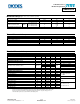
A
Product Line o
f
Diodes Incorporated
DMN2300UFB
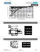
Maximum Ratings @T
A
= 25°C unless otherwise specified
Characteristic Symbol Value Unit
Drain-Source Voltage
V
DSS
20 V
Gate-Source Voltage
V
GSS
±8 V
Continuous Drain Current
Steady
State
T
A
= 25°C (Note 4)
T
A
= 85°C (Note 4)
T
A
= 25°C (Note 5)
I
D
1.32
0.94
1.78
A
Pulsed Drain Current (Note 6)
I
DM
8 A
Thermal Characteristics @T
A
= 25°C unless otherwise specified
Characteristic Symbol Value Unit
Power Dissipation (Note 4)
P
D
0.468 W
Power Dissipation (Note 5)
P
D
1.2 W
Thermal Resistance, Junction to Ambient (Note 4)
R
θJA
267 °C/W
Thermal Resistance, Junction to Ambient (Note 5)
R
θJA
104 °C/W
Operating and Storage Temperature Range
T
J
, T
STG
-55 to +150 °C
Electrical Characteristics @T
A
= 25°C unless otherwise specified
Characteristic Symbol Min Typ Max Unit Test Condition
OFF CHARACTERISTICS (Note 7)
Drain-Source Breakdown Voltage
BV
DSS
20 - - V
V
GS
= 0V, I
D
= 10μA
Zero Gate Voltage Drain Current T
J
= 25°C I
DSS
- - 1
μA
V
DS
= 20V, V
GS
= 0V
Gate-Source Leakage
I
GSS
- - 10
μA
V
GS
= ±8V, V
DS
= 0V
ON CHARACTERISTICS (Note 7)
Gate Threshold Voltage
V
GS
(
th
)
0.45 - 0.95 V
V
DS
= V
GS
, I
D
= 250μA
Static Drain-Source On-Resistance
R
DS (ON)
- - 175
mΩ
V
GS
= 4.5V, I
D
= 300mA
- - 240
V
GS
= 2.5V, I
D
= 250mA
- - 360
V
GS
= 1.8V, I
D
= 100mA
Forward Transfer Admittance
|Y
fs
|
40 - - mS
V
DS
= 3V, I
D
= 30mA
Diode Forward Voltage
V
SD
- 0.7 1.2 V
V
GS
= 0V, I
S
= 300mA
DYNAMIC CHARACTERISTICS
Input Capacitance
C
iss
- 67.62 -
pF
V
DS
= 20V, V
GS
= 0V,
f = 1.0MHz
Output Capacitance
C
oss
- 9.74 -
pF
Reverse Transfer Capacitance
C
rss
- 7.58 -
pF
Gate Resistance
R
g
- 68.51 -
Ω
V
DS
= 0V, V
GS
= 0V, f = 1MHz
Total Gate Charge
Q
g
- 0.89 -
nC
V
GS
= 4.5V, V
DS
= 10V,
I
D
= 1A
Gate-Source Charge
Q
g
s
- 0.14 -
nC
Gate-Drain Charge
Q
g
d
- 0.16 -
nC
Turn-On Delay Time
t
D
(
on
)
- 4.92 -
ns
V
DS
= 10V, I
D
= 1A
V
GS
= 4.5V, R
G
= 6Ω
Turn-On Rise Time
t
r
- 6.93 -
ns
Turn-Off Delay Time
t
D
(
off
)
- 21.71 -
ns
Turn-Off Fall Time
t
f
- 10.62 -
ns
Notes: 4. Device mounted on FR-4 substrate PC board, 2oz copper, with minimum recommended pad layout
5. Device mounted on FR-4 substrate PC board, 2oz copper, with 25mm X 25mm square copper plate
6. Device mounted on minimum recommended pad layout test board, 10μs pulse duty cycle = 1%.
7. Short duration pulse test used to minimize self-heating effect.