
Manual


DMN26D0UFB4
Document number: DS31775 Rev. 7 - 2
1 of 6
www.diodes.com
March 2012
© Diodes Incorporated
DMN26D0UFB4
N-CHANNEL ENHANCEMENT MODE MOSFET
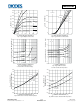
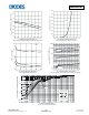
Product Summary
V
(BR)DSS
R
DS(on)
I
D
T
A
= 25°C
20V
3.0Ω @ V
GS
= 4.5V
240mA
6.0Ω @ V
GS
= 1.8V
170mA
Description and Applications
This new generation MOSFET has been designed to minimize the on-
state resistance (R
DS(on)
) and yet maintain superior switching
performance, making it ideal for high efficiency power management
applications.
• DC-DC Converters
• Power management functions
Features and Benefits
• N-Channel MOSFET
• Low On-Resistance:
• 3.0 Ω @ 4.5V
• 4.0 Ω @ 2.5V
• 6.0 Ω @ 1.8V
• 10 Ω @ 1.5V
• Very Low Gate Threshold Voltage, 1.05V max
• Low Input Capacitance
• Fast Switching Speed
• Low Input/Output Leakage
• Ultra-Small Surface Mount Package, 0.4mm Maximum Package
Height
• ESD Protected Gate
• Lead, Halogen and Antimony Free, RoHS Compliant (Note 1)
• "Green" Device (Note 2)
• Qualified to AEC-Q101 Standards for High Reliability
Mechanical Data
• Case: X2-DFN1006-3
• Case Material: Molded Plastic, “Green” Molding Compound. UL
Flammability Classification Rating 94V-0
• Moisture Sensitivity: Level 1 per J-STD-020
• Terminal Connections: See Diagram
• Terminals: Finish – NiPdAu over Copper leadframe. Solderable
per MIL-STD-202, Method 208
• Weight: 0.001 grams (approximate)
Ordering Information (Note 3)
Part Number Case Packaging
DMN26D0UFB4-7 X2-DFN1006-3 3,000/Tape & Reel
DMN26D0UFB4-7B X2-DFN1006-3 10,000/Tape & Reel
Notes: 1. No purposefully added lead.
2.
Diodes Inc.’s “Green” policy can be found on our website at http://www.diodes.com.
3. For packaging details, go to our website at http://www.diodes.com.
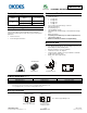
Marking Information
X2-DFN1006-3
Bottom View
Equivalent Circuit
To
p
View
Source
Body
Diode
Gate
Protection
Diode
Gate
Drai
n
D
S
G
ESD PROTECTED
DMN26D0UFB4-7BDMN26D0UFB4-7
Top View
Dot Denotes Drain Side
Top View
Bar Denotes Gate
and Source Side
M1 = Product Type Marking Code
M1
M1