
Owner's manual

DMN601DWK
Document number: DS30656 Rev. 7 - 2
1 of 5
www.diodes.com
January 2014
© Diodes Incorporated
DMN601DW
K
NEW PRODUCT
DUAL N-CHANNEL ENHANCEMENT MODE FIELD EFFECT TRANSISTOR
Product Summary
V
(BR)DSS
R
DS(ON)
max
I
D
max
T
A
= +25°C
60V
3 @ V
GS
= 5V
0.3A
Description
This MOSFET has been designed to minimize the on-state resistance
(R
DS(ON)
) and yet maintain superior switching performance, making it
ideal for high efficiency power management applications.
Applications
Motor Control
Power Management Functions
Features
Dual N-Channel MOSFET
Low On-Resistance
Low Gate Threshold Voltage
Low Input Capacitance
Fast Switching Speed
Low Input/Output Leakage
Ultra-Small Surface Mount Package
ESD Protected Up To 2kV
Totally Lead-Free & Fully RoHS Compliant (Notes 1 & 2)
Halogen and Antimony Free. “Green” Device (Note 3)
Qualified to AEC-Q101 Standards for High Reliability
Mechanical Data
Case: SOT363
Case Material: Molded Plastic. “Green” Molding Compound.
UL Flammability Classification Rating 94V-0
Moisture Sensitivity: Level 1 per J-STD-020
Terminals: Matte Tin Finish annealed over Alloy 42 leadframe
(Lead Free Plating). Solderable per MIL-STD-202, Method 208
Terminal Connections: See Diagram
Weight: 0.006 grams (approximate)
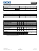
Ordering Information (Note 4)
Part Number Case Packaging
DMN601DWK-7 SOT-363 3000/Tape & Reel
Notes: 1. No purposely added lead. Fully EU Directive 2002/95/EC (RoHS) & 2011/65/EU (RoHS 2) compliant.
2. See http://www.diodes.com/quality/lead_free.html for more information about Diodes Incorporated’s definitions of Halogen- and Antimony-free, "Green"
and Lead-free.
3. Halogen- and Antimony-free "Green” products are defined as those which contain <900ppm bromine, <900ppm chlorine (<1500ppm total Br + Cl) and
<1000ppm antimony compounds.
4. For packaging details, go to our website at http://www.diodes.com/products/packages.html.
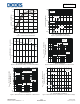
Marking Information
Date Code Key
Year 2005 2006 2007 2008 2009 2010 2011 2012 2013 2014 2015 2016 2017
Code S T U V W X Y Z A B C D E
Month Jan Feb Mar Apr May Jun Jul Aug Sep Oct Nov Dec
Code 1 2 3 4 5 6 7 8 9 O N D
SOT363
Top View
S
1
D
1
D
2
S
2
G
1
G
2
ESD Protected up to 2kV
Source
Body
Diode
EQUIVALENT CIRCUIT PER ELEMENT
Gate
Protection
Diode
Gate
Drai
n
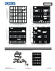
K7K YM
S
1
D
2
G
1
D
1
S
2
G
2
K7K YM
Top View
Internal Schematic
K7K YM
S
1
D
2
G
1
D
1
S
2
G
2
K7K YM
K7K = Product Type Marking Code
YM = Date Code Marking for SAT (Shanghai Assembly/ Test site)
YM = Date Code Marking for CAT (Chengdu Assembly/ Test site)
Y or Y = Year (ex: A = 2013)
M = Month (ex: 9 = September)